CMOS power amplifier

A technology of power amplifiers and amplifiers, which is applied in the direction of power amplifiers, amplifiers, amplification control, etc.

Active Publication Date: 2012-02-08
SAMSUNG ELECTRO MECHANICS CO LTD
View PDF5 Cites 6 Cited by
  • Summary
  • Abstract
  • Description
  • Claims
  • Application Information

AI Technical Summary

Problems solved by technology

That is, to amplify different signals, two different amplifiers must be purchased

Method used


Image

  • CMOS power amplifier
  • CMOS power amplifier
  • CMOS power amplifier

Examples


Embodiment Construction

[0029] Exemplary embodiments of the present invention will be described in detail with reference to the accompanying drawings. However, this invention may be embodied in many different forms and should not be construed as limited to the embodiments set forth herein. Rather, these embodiments are provided so that this disclosure will be thorough and complete, and will fully convey the scope of the invention to those skilled in the art. In the drawings, the shapes and dimensions may be exaggerated for clarity, and the same reference numerals will be used throughout to designate the same or like elements.

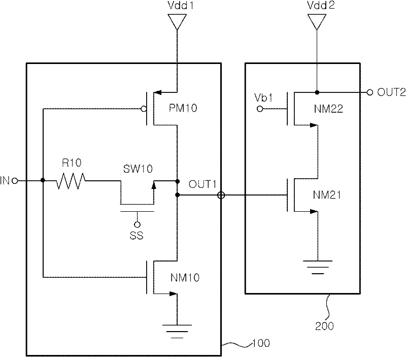
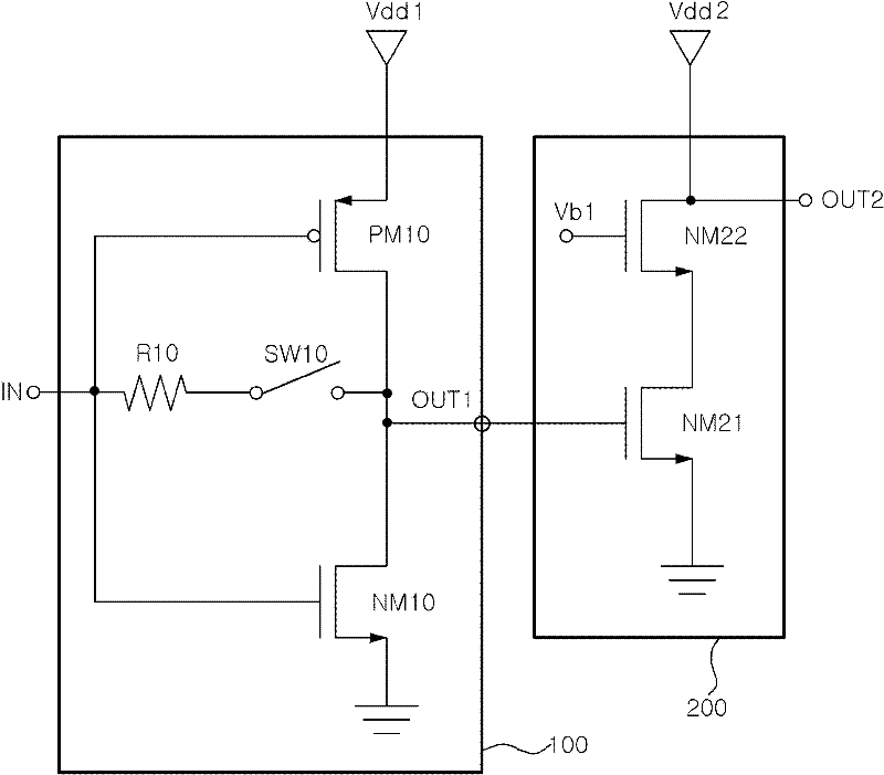
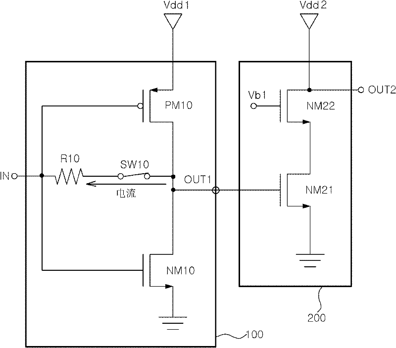
[0030] figure 1 is a circuit diagram of a CMOS power amplifier according to an exemplary embodiment of the present invention.

[0031] refer to figure 1 , The CMOS power amplifier according to the exemplary embodiment of the present invention may include: a driver stage 100 for receiving a first power supply (power) Vdd1 and amplifying an input signal; and a power stage 200...


PUM


Abstract

A CMOS power amplifier includes: a first MOS transistor connected between a first power terminal and a first output stage and having a gate connected to an input stage; a second MOS transistor connected between the first output stage and a ground and having a gate connected to the input stage; a switching circuit unit connecting or separating a feedback line between the input stage and the first output stage to select a linear amplifying operation or a non-linear amplifying operation; and a resistor formed at the feedback line between the input stage and the first output stage to determine a linear amplification gain when the feedback line is turned on.

Description

[0001] Cross References to Related Applications [0002] This application claims priority from Korean Patent Application No. 10-2010-0073640 filed with the Korean Intellectual Property Office on Jul. 29, 2010, the disclosure of which is hereby incorporated by reference. technical field [0003] The present invention relates to a CMOS power amplifier applicable to a front-end module, and more particularly, to a CMOS power amplifier which can be selectively used as a nonlinear amplifier or a linear amplifier by adjusting its amplification gain. Background technique [0004] In general, nearly 80% of the mobile phone demands in the world are GSM (Global System for Mobile Communications) phones using nonlinear signals. It is expected that EDGE or W-CDMA phones using linear signals will be widely used in the future market. popular and used. [0005] Therefore, for a single power amplifier, an amplifier capable of selectively amplifying GSM signals and EDGE / W-CDMA signals is requ...

Claims


Application Information

Patent Timeline
Patent Type & Authority Applications(China)
IPC IPC(8): H03F3/20H03G3/20
CPCH03F1/223H03F3/245H03F3/3028H03F2200/249H03F2200/411H03F2200/516H03F2203/30031H03G1/0088
Inventor 金胤锡尹喆焕南重镇金基仲元俊九
Owner SAMSUNG ELECTRO MECHANICS CO LTD
Why Eureka
Try Eureka