Device with through-silicon via (tsv) and method of forming the same

A device, silicon substrate technology, used in semiconductor devices, electric solid state devices, semiconductor/solid state device manufacturing, etc.

Active Publication Date: 2012-04-18
TAIWAN SEMICON MFG CO LTD
View PDF3 Cites 16 Cited by
  • Summary
  • Abstract
  • Description
  • Claims
  • Application Information

AI Technical Summary

Problems solved by technology

Sidewall insulation roughness is ...

Method used


Image

  • Device with through-silicon via (tsv) and method of forming the same
  • Device with through-silicon via (tsv) and method of forming the same
  • Device with through-silicon via (tsv) and method of forming the same

Examples


Embodiment Construction

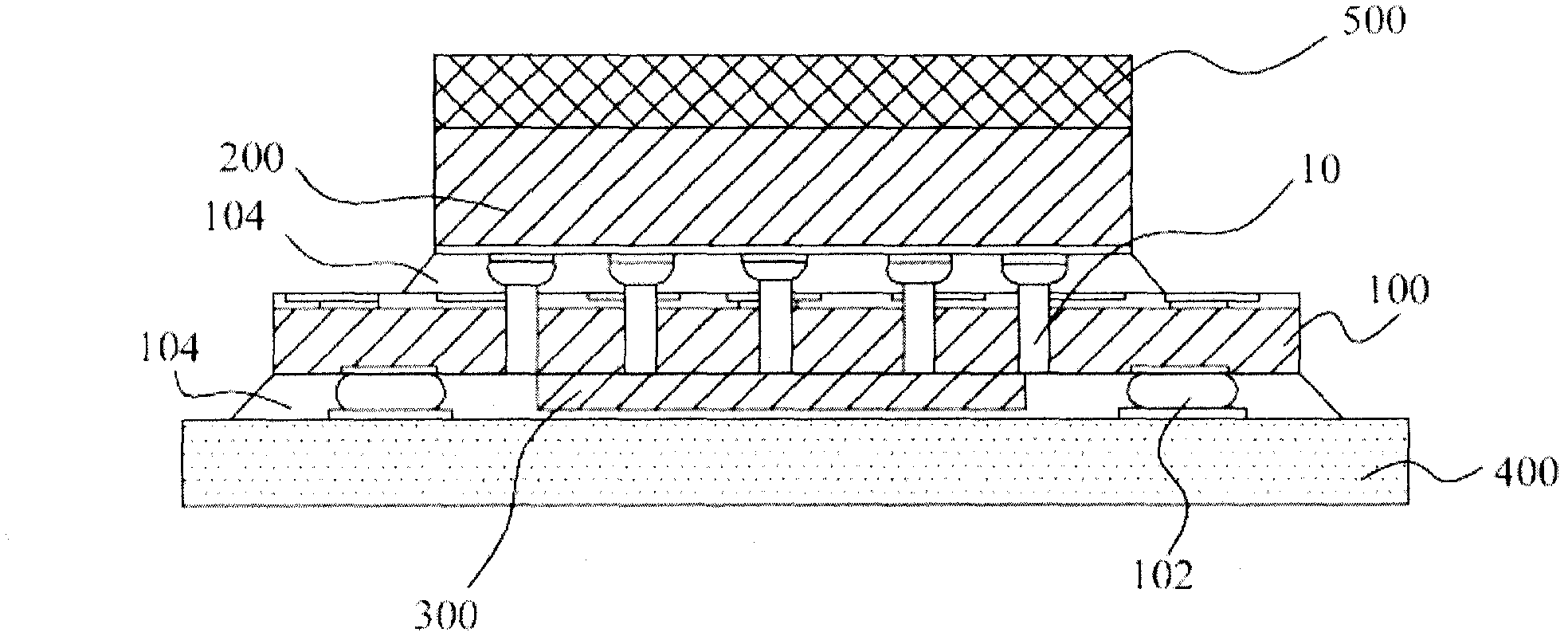
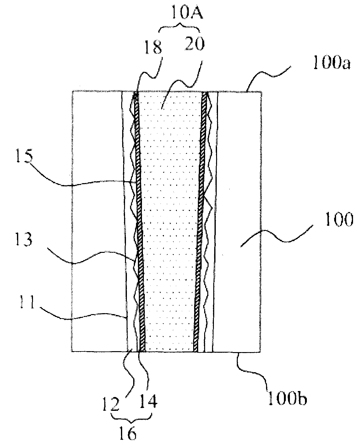
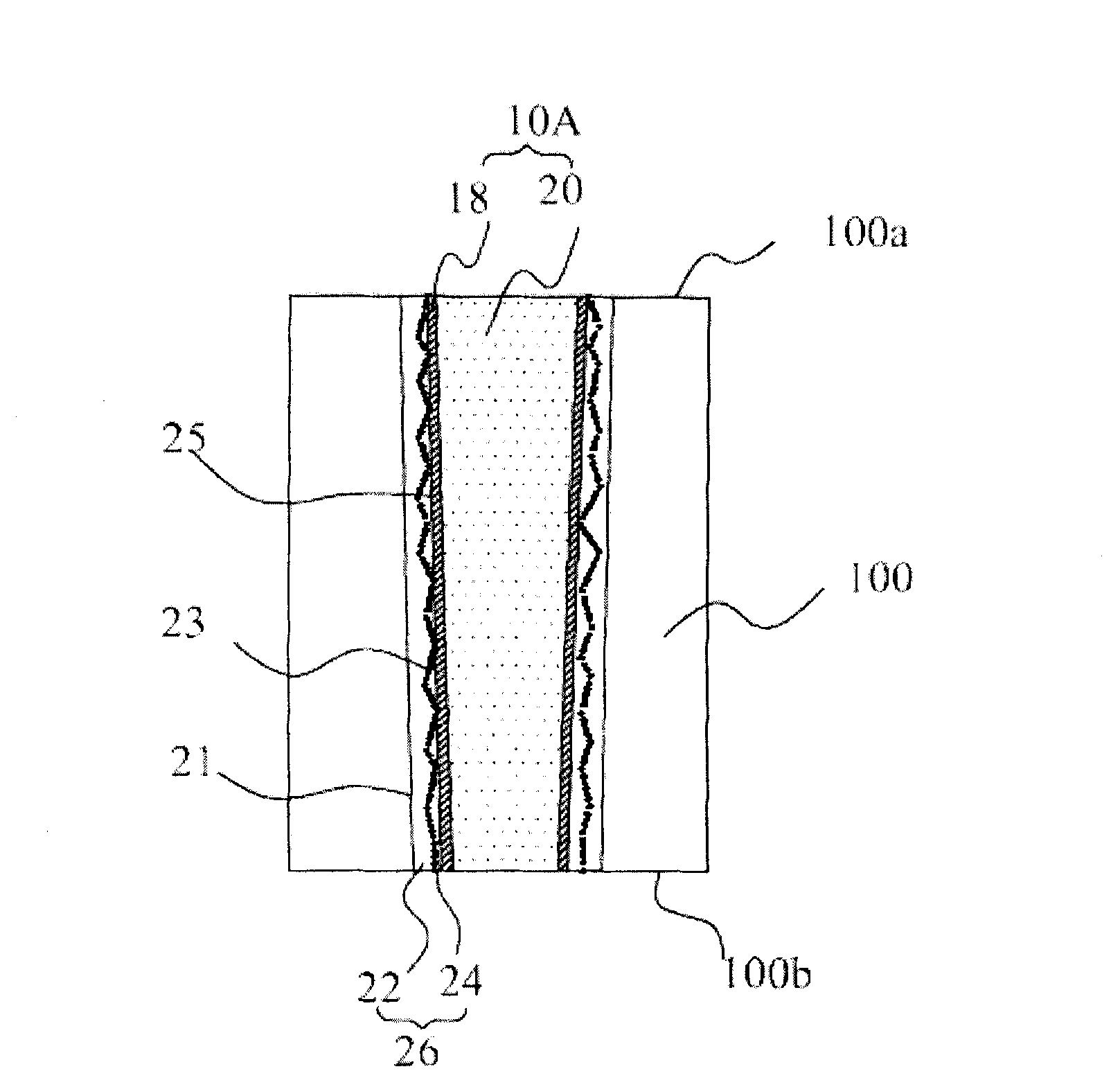
[0029] The present disclosure provides embodiments of TSVs with sidewall insulation and processes for forming the same. TSVs with sidewall insulation can be fabricated on wafers, IC dies, interposers, or substrates for flip-chip assembly, wafer-level chip-scale packaging (WLCSP), three-dimensional integrated circuit (3D-IC) stacking, and / or Or any advanced packaging technology field. Exemplary embodiments shown in the drawings will now be described in detail. Wherever possible, the same reference numbers are used in the drawings and description to refer to the same or like parts. In the drawings, shapes and thicknesses may be exaggerated for clarity and convenience. The description is particularly directed to elements forming part of, or cooperating directly with, an apparatus according to the present disclosure. It is to be understood that elements not specifically shown or described may take any form known in the art. Also, when a layer is referred to as being on another...


PUM


Abstract

A device with through-silicon via (TSV) and a method of forming the same includes the formation of an opening in a silicon substrate, the formation of a first insulation layer on the sidewalls and bottom of the opening, the formation of a second insulation layer on the sidewalls and bottom of the opening. A first interface between the first insulation layer and the silicon substrate has an interface roughness with a peak-to-valley height less than 5 nm. A second interface between the second insulation layer and the conductive layer has an interface roughness with a peak-to-valley height less than 5 nm.

Description

technical field [0001] The present invention relates to integrated circuit fabrication, and more particularly, to through-silicon via (TSV) fabrication. Background technique [0002] Three-dimensional system-in-package (3D-SiP) technology is driven by the strong demand for high-speed, high-density, small-size, and multifunctional electronic devices. Through-silicon-via (TSV) interconnection is popular as a form of 3D integration due to its shorter interconnection distance and faster speed. To address the need for flip-chip packaging technology, silicon (Si) interposers with TSVs have been proposed as a means of providing high write density interconnects, enabling interposers between die and interposer due to short interconnects from chip to substrate. A good solution for minimizing the coefficient of thermal expansion (CTE) mismatch and improving electronic performance. There are multiple steps involved in the TSV process that can successfully address packaging technology ...

Claims


Application Information

Patent Timeline
IPC IPC(8): H01L23/522H01L21/768
CPCH01L21/76831H01L23/3121H01L21/486H01L2224/73204H01L2225/06517H01L2224/32225H01L21/563H01L25/0657H01L23/147H01L2224/16235H01L2225/0652H01L2225/06541H01L21/76898H01L2224/16225H01L23/49816H01L2225/06513H01L2225/06572H01L23/481H01L23/49827H01L2924/00
Inventor 余振华邱文智廖鄂斌吴仓聚
Owner TAIWAN SEMICON MFG CO LTD
Why Eureka
Try Eureka