Electronic device shell and manufacturing method thereof

A technology of electronic devices and manufacturing methods, which is applied in the fields of electrical equipment casings/cabinets/drawers, decorative arts, electrical components, etc., and can solve the problems that the important functions of signs cannot be effectively exerted, are easily damaged by wear, and lack metal texture, etc.

Inactive Publication Date: 2012-05-09
SHENZHEN FUTAIHONG PRECISION IND CO LTD
View PDF2 Cites 18 Cited by
  • Summary
  • Abstract
  • Description
  • Claims
  • Application Information

AI Technical Summary

Problems solved by technology

Marks formed by inks and paints have poor abrasion resistance and are easily damaged by abrasion
Moreover, the signs formed by ink and paint are often difficult to attract consumers' attention because of insufficient brightness and lack of metallic texture, so that the important functions of the signs cannot be effectively brought into play

Method used


Image

  • Electronic device shell and manufacturing method thereof
  • Electronic device shell and manufacturing method thereof

Examples


Embodiment Construction

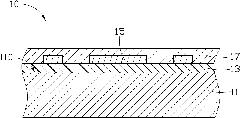
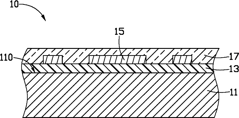
[0022] see figure 1 , the electronic device casing 10 of the preferred embodiment of the present invention includes a substrate 11 , a primer layer 13 , a metallic vacuum coating layer 15 and a transparent topcoat layer 17 . The vacuum coating layer 15 forms patterns on the housing 10 of the electronic device, such as logos, graphics and characters.

[0023] The base body 11 is made of plastic. The primer layer 13 is formed on the outer surface 110 of the substrate 11 . The primer layer 13 is used to increase the adhesion of the vacuum coating layer 15 . The thickness of the primer layer 13 is about 6-12 μm.

[0024] The vacuum coating layer 15 is formed on the primer layer 13 . In order not to affect the radio frequency transmitting and receiving functions of the electronic device using the electronic device case 10 , the vacuum coating layer 15 can be a non-conductive discontinuous coating layer with a metallic appearance. Preferably, the color of the vacuum coating lay...


PUM

PropertyMeasurementUnit
thicknessaaaaaaaaaa

Abstract

The invention provides an electronic device shell which comprises a plastic matrix, a primer layer, a metal color vacuum coating layer and a transparent finish paint layer, wherein the primer layer is formed on the outer surface of the matrix; the vacuum coating layer is formed on the primer layer; a pattern is formed on the vacuum coating layer and on the electronic device shell; and the finish paint layer is formed on the vacuum coating layer and on the primer layer which is not covered by the vacuum coating layer. The invention also provides a method for manufacturing the electronic device shell. The pattern such as a mark, the pattern or characters on the surface of the electronic device shell not only has high luminance brightness, but also has metal texture and has an obvious visual effect.

Description

technical field [0001] The invention relates to an electronic device casing and a manufacturing method thereof. Background technique [0002] Equipment signs, such as trademarks, models, or special graphics or characters, are generally placed at prominent positions on the surface of the housing of the electronic device for user identification or for advertising purposes. For example, the business logo on the top of the mobile phone display will be designed as eye-catching and beautiful as possible to highlight the quality and strength of the business, attract consumers' attention, and win consumer recognition. [0003] However, compared with the electronic device itself, the marks on the surface of the housing are generally smaller, and are generally formed by printing ink or spraying paint. Marks formed by inks and paints have poor abrasion resistance and are easily damaged by abrasion. Moreover, the signs formed by ink and paint are often difficult to attract consumers' ...

Claims


Application Information

Patent Timeline
Patent Type & Authority Applications(China)
IPC IPC(8): H05K5/00B44C5/04
CPCB44C1/227Y10T428/13Y10T428/1359
Inventor 王世峰陈冠宏
Owner SHENZHEN FUTAIHONG PRECISION IND CO LTD
Why Eureka
Try Eureka