Controlling an electronic device using chiplets
A technology of small chips and optoelectronic devices, applied in the direction of electric solid devices, electrical components, semiconductor devices, etc., can solve the problems of testing pixel control circuits of displays, discarding faulty devices, and inability to correct circuits.
- Summary
- Abstract
- Description
- Claims
- Application Information
AI Technical Summary
Problems solved by technology
Method used
Image

Examples
Embodiment Construction
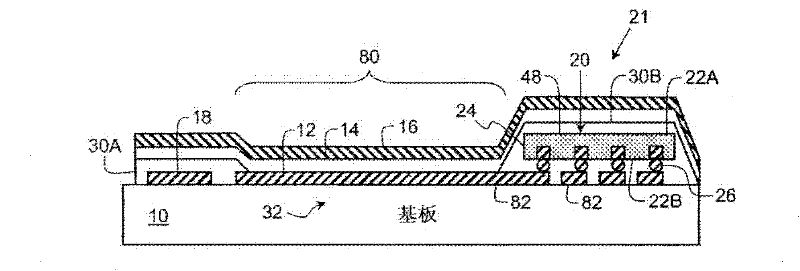
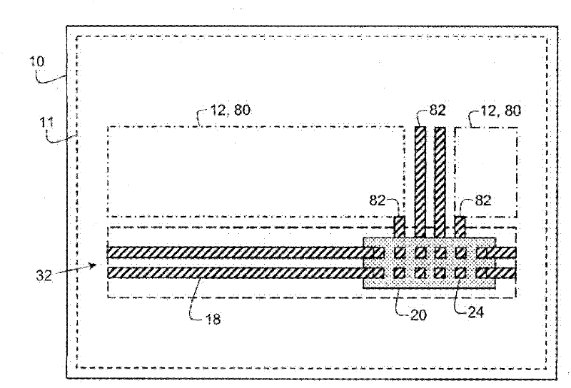
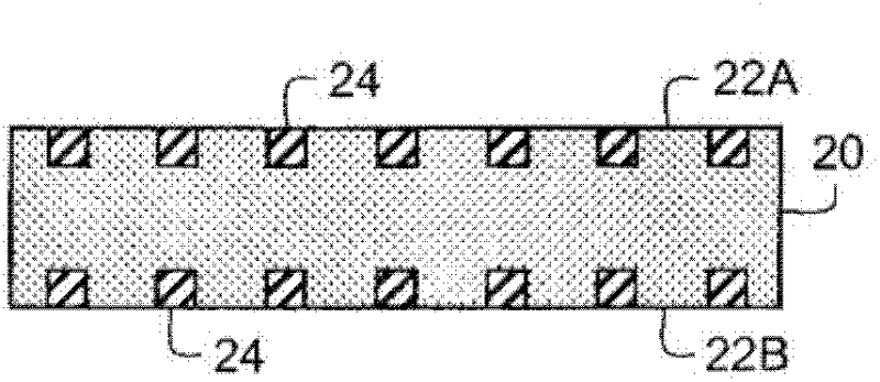
[0027] refer to figure 1 and figure 2 , in one embodiment of the invention, an electronic device includes a common substrate 10 having an optical working area 11 , wherein a plurality of chiplet sites 21 are located in the working area 11 on the common substrate 10 . A plurality of controlled optoelectronic devices 80 are located in the working area 11 on a common substrate 10 , each optoelectronic device is adapted to emit or absorb light, and a wiring layer 32 with a plurality of conductors 18 is formed on the common substrate 10 . These conductors may include, for example, metals, conductive metal oxides, or conductive polymers. A plurality of chiplets 20 are located on common substrate 10 in chiplet locations 21, each chiplet 20 having an individual substrate 48 separate from common substrate 10, each individual substrate 48 having a top surface opposite bottom surface 22B 22A, and one or more connection pads 24 are formed on the bottom surface 22B of the chiplet 20. E...
PUM
 Abstract
Description
Claims
Application Information
 - R&D
- Intellectual Property
- Life Sciences
- Materials
- Tech Scout
- Unparalleled Data Quality
- Higher Quality Content
- 60% Fewer Hallucinations
Browse by: Latest US Patents, China's latest patents, Technical Efficacy Thesaurus, Application Domain, Technology Topic, Popular Technical Reports.
© 2025 PatSnap. All rights reserved.Legal|Privacy policy|Modern Slavery Act Transparency Statement|Sitemap|About US| Contact US: help@patsnap.com