Supercharge Your Innovation With Domain-Expert AI Agents!

SET (Single-Electron Transistor)/CMOS (Complementary Metal-Oxide-Semiconductor Transistor) inverter based on negative differential resistance property

A technology of negative differential resistance and inverter, applied in the direction of logic circuit connection/interface layout, logic circuit coupling/interface using field effect transistors, etc., can solve the problem of high transmission delay, limited application range, and cannot achieve full output voltage swing Amplitude and other issues to achieve the effect of reducing transmission delay and low power consumption

Active Publication Date: 2014-05-07
FUZHOU UNIV
View PDF2 Cites 0 Cited by
  • Summary
  • Abstract
  • Description
  • Claims
  • Application Information

AI Technical Summary

Problems solved by technology

However, the currently proposed hybrid SET / CMOS inverter has the disadvantages of high propagation delay and inability to achieve full output voltage swing, which limits its application range.

Method used


Image

  • SET (Single-Electron Transistor)/CMOS (Complementary Metal-Oxide-Semiconductor Transistor) inverter based on negative differential resistance property
  • SET (Single-Electron Transistor)/CMOS (Complementary Metal-Oxide-Semiconductor Transistor) inverter based on negative differential resistance property
  • SET (Single-Electron Transistor)/CMOS (Complementary Metal-Oxide-Semiconductor Transistor) inverter based on negative differential resistance property

Examples


Embodiment Construction

[0014] The present invention will be further described below in conjunction with the drawings and embodiments.

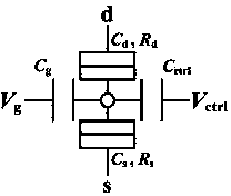
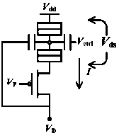
[0015] This embodiment provides a SET / CMOS inverter based on negative differential resistance characteristics, which is characterized by including a single-electron transistor SET, a PMOS tube, and an NMOS tube, wherein the single-electron transistor SET is passed through two tunnel junctions. The Coulomb islands are connected in series, and the applied bias voltage is coupled to the Coulomb islands by the gate capacitance. The source of the PMOS tube is connected to the source of the single-electron transistor SET, and the gate of the single-electron transistor SET is connected to the PMOS tube. The drain is connected, the drain of the NMOS tube is connected to the drain of the PMOS tube, and the source of the NMOS tube is grounded.

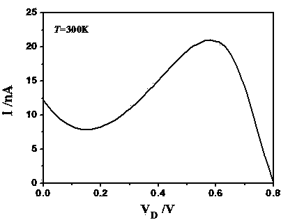
[0016] The negative differential resistance characteristic of the above-mentioned single-electron transistor SET connected with PMOS and ...


PUM


Abstract

The invention relates to an SET (Single-Electron Transistor) / CMOS (Complementary Metal-Oxide-Semiconductor Transistor) inverter based on a negative differential resistance property, which is characterized by comprising an SET, a PMOS (P-channel Metal Oxide Semiconductor) tube and an NMOS (N-channel Metal Oxide Semiconductor) tube. The source electrode of the PMOS tube is connected with the source electrode of the SET, the grid electrode of the SET is connected with the drain electrode of the PMOS tube, and the drain electrode of the NMOS tube is connected with the drain electrode of the PMOS tube. According to the SET / CMOS inverter based on the negative differential resistance property provided by the invention, the power consumption is low, and the full swing of the output voltage and the lower transmission delay can be realized, so that the SET / CMOS inverter can be applied to the digital circuit design well.

Description

Technical field [0001] The invention relates to a SET / CMOS inverter based on negative differential resistance characteristics. Background technique [0002] When the characteristic size of the MOS tube enters 100nm with the development of Moore's Law, its reliability and electrical characteristics are faced with many challenges due to the influence of quantum effects. Single-electron transistor (SET), as a new type of nanoelectronic device, is expected to become a powerful substitute for MOS tube after entering the nanometer field. SET is composed of Coulomb island, gate capacitance and two tunneling structures. It mainly controls electron tunneling through gate voltage to form current, and has ultra-small size and extremely low power consumption. In addition, single-electron transistors also have unique Coulomb blocking oscillation characteristics and higher charge sensitivity, which can effectively reduce the complexity of the circuit. However, due to the shortcomings of high...

Claims


Application Information

Patent Timeline
Patent Type & Authority Patents(China)
IPC IPC(8): H03K19/0185
Inventor 魏榕山陈寿昌陈锦锋何明华
Owner FUZHOU UNIV
Features
  • R&D
  • Intellectual Property
  • Life Sciences
  • Materials
  • Tech Scout
  • Unparalleled Data Quality
  • Higher Quality Content
  • 60% Fewer Hallucinations
Learn More