Split gate semiconductor device with curved gate oxide profile

A gate oxide layer and semiconductor technology, applied in semiconductor devices, semiconductor/solid-state device manufacturing, electrical components, etc., can solve the problems of difficult etching rate, affecting device on-resistance input capacitance, affecting the uniformity of isolation layer, etc.

Active Publication Date: 2012-09-05
VISHAY SILICONIX LLC
View PDF4 Cites 19 Cited by
  • Summary
  • Abstract
  • Description
  • Claims
  • Application Information

AI Technical Summary

Problems solved by technology

However, achieving consistent etch rates for dielectrics and oxides can be difficult
Differences in etch rate can affect

Method used


Image

  • Split gate semiconductor device with curved gate oxide profile
  • Split gate semiconductor device with curved gate oxide profile
  • Split gate semiconductor device with curved gate oxide profile

Examples


Embodiment Construction

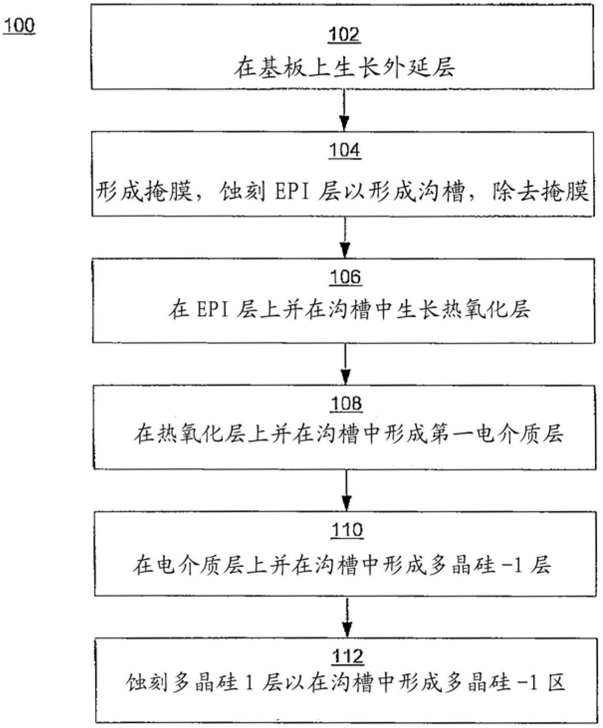
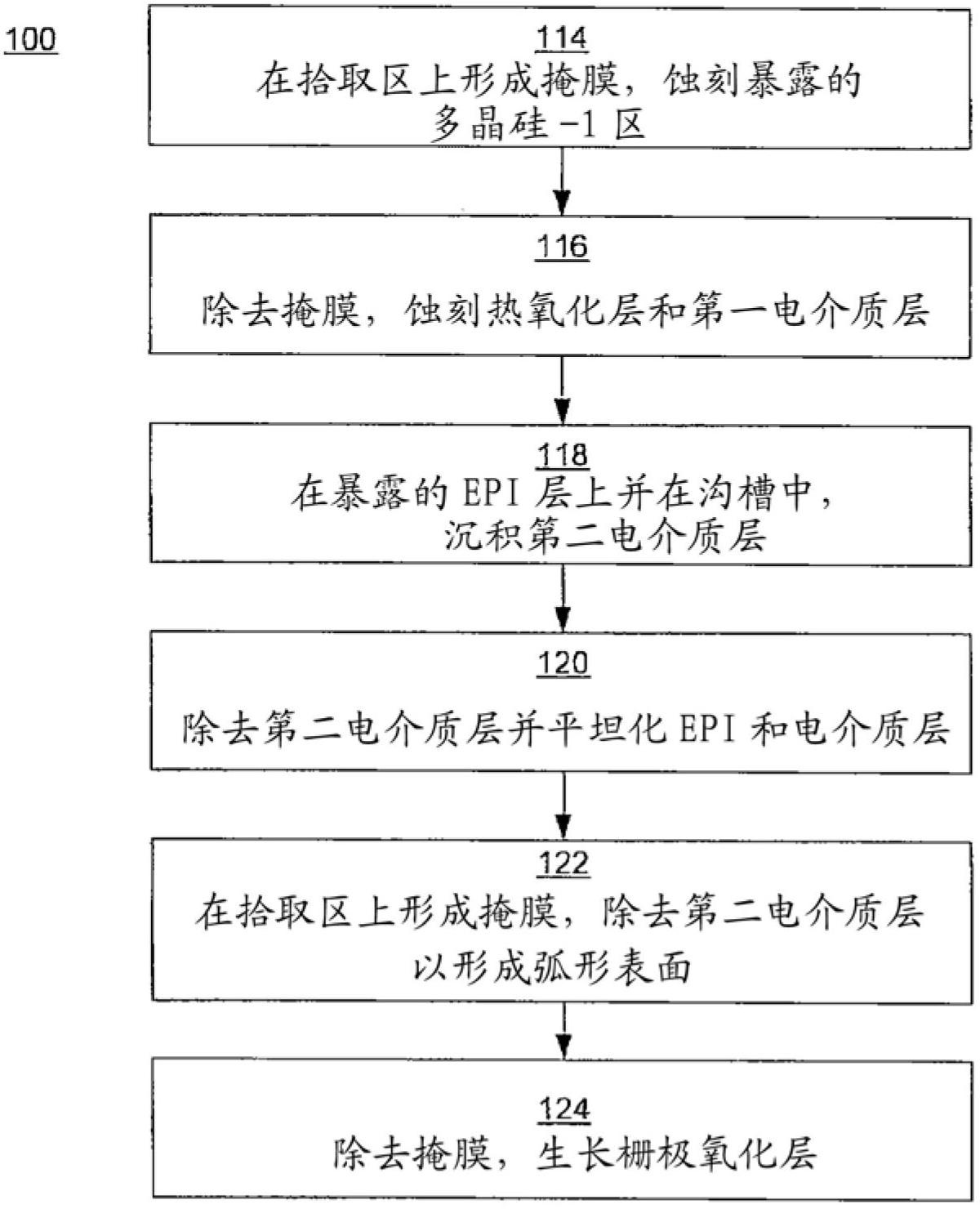
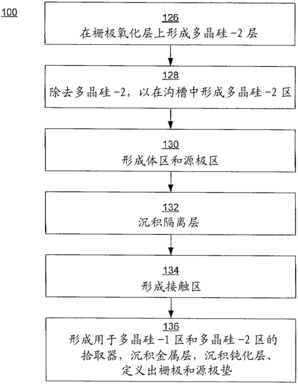
[0015] In the following detailed description of the invention, numerous specific details are set forth in order to provide a thorough understanding of the invention. However, one skilled in the art will recognize that the invention may be practiced without these specific details or with their equivalents. In other instances, well-known methods, procedures, components, and circuits have not been described in detail so as not to unnecessarily obscure aspects of the invention.

[0016] Some portions of the detailed description below will be expressed in terms of procedures, logical blocks, processes, and other symbolic representations of operations for fabricating a semiconductor device. These descriptions and representations are the means used by those skilled in the art of semiconductor device fabrication to most effectively convey the substance of their work to others skilled in the art. In this application, a procedure, box, process, or the like, is considered to be a self-c...


PUM


Abstract

A split gate semiconductor device includes a trench gate having a first electrode region and a second electrode region that are separated from each other by a gate oxide layer and an adjacent dielectric layer. The boundary of the gate oxide layer and the dielectric layer is curved to avoid a sharp corner where the gate oxide layer meets the sidewalls of the trench.

Description

technical field [0001] Embodiments according to the present invention generally pertain to semiconductor devices. Background technique [0002] To save power, it is important to reduce power loss in transistors. In metal-oxide-semiconductor field-effect transistor (MOSFET) devices, and especially in the MOSFET class known as power MOSFETs, power loss can be reduced by reducing the drain-to-source on-resistance (Rdson) of the device. [0003] Split-gate power MOSFETs, also known as shielded-gate trench MOSFETs, take advantage of larger doping concentrations in the epitaxial layer to reduce Rdson. A split-gate power MOSFET incorporates a trenched gate comprising a first electrode (e.g. polysilicon, or polysilicon-1) connected to a second electrode (e.g. , polysilicon, or polysilicon-2) separately. Properly forming the isolation layer can be challenging from a manufacturing standpoint. [0004] In one conventional fabrication process, a spacer layer is grown on the exposed ...

Claims


Application Information

Patent Timeline
IPC IPC(8): H01L29/78H01L21/336
CPCH01L29/407H01L29/66727H01L29/66734H01L29/7811H01L29/7813H01L29/0615H01L29/0623H01L29/0696H01L29/66621
Inventor Y.高K-I.陈K.特里尔S.史
Owner VISHAY SILICONIX LLC
Why Eureka
Try Eureka