Structure and method of flip chip encapsulation of non-array bumps

A bump and molding technology, applied in semiconductor/solid-state device manufacturing, electrical components, electrical solid-state devices, etc., can solve the problems of thermal expansion, bursting, and slow filling of chips and substrates, and achieve the effect of slowing down the speed of mold flow.

Inactive Publication Date: 2014-10-29
POWERTECH TECHNOLOGY INC
View PDF4 Cites 0 Cited by
  • Summary
  • Abstract
  • Description
  • Claims
  • Application Information

AI Technical Summary

Problems solved by technology

This process has the following disadvantages: (1) Filling is slow. Driven by capillary action, the filling time is approximately proportional to the square of the distance, and the filling time is about a few minutes to ten minutes depending on the temperature of the underfill. ; (2) A set of primer filling equipment can only dispense glue on a single chip at a time. If two (including) chips are to be dispensed at the same time, it is necessary to prepare multiple sets of glue dispensing equipment, which will increase the burden of cost
Such a semiconductor packaging product with air holes or air bubbles will weaken the mechanical strength of the product
Moreover, when there are air bubbles or air holes in the molding compound, it is easy to cause thermal expansion between the chip and the substrate during the thermal cycle process and burst, resulting in problems such as quality reliability (reliability)

Method used


Image

  • Structure and method of flip chip encapsulation of non-array bumps
  • Structure and method of flip chip encapsulation of non-array bumps
  • Structure and method of flip chip encapsulation of non-array bumps

Examples


Embodiment Construction

[0037] Hereinafter, the embodiments of the present invention will be described in detail with the accompanying drawings. However, it should be noted that the drawings are simplified schematic diagrams, and the basic structure or implementation methods of the present invention are illustrated only by schematic methods, so they are only shown related to the present invention. The elements and combination relationships of are not used to limit the present invention.

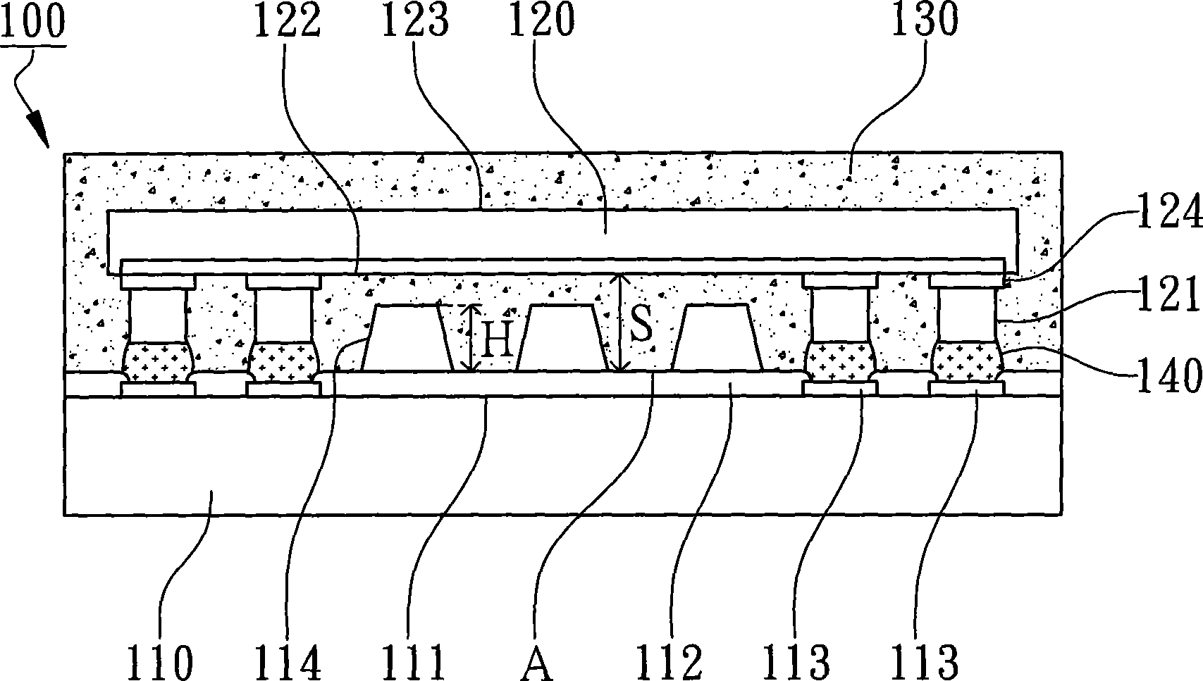
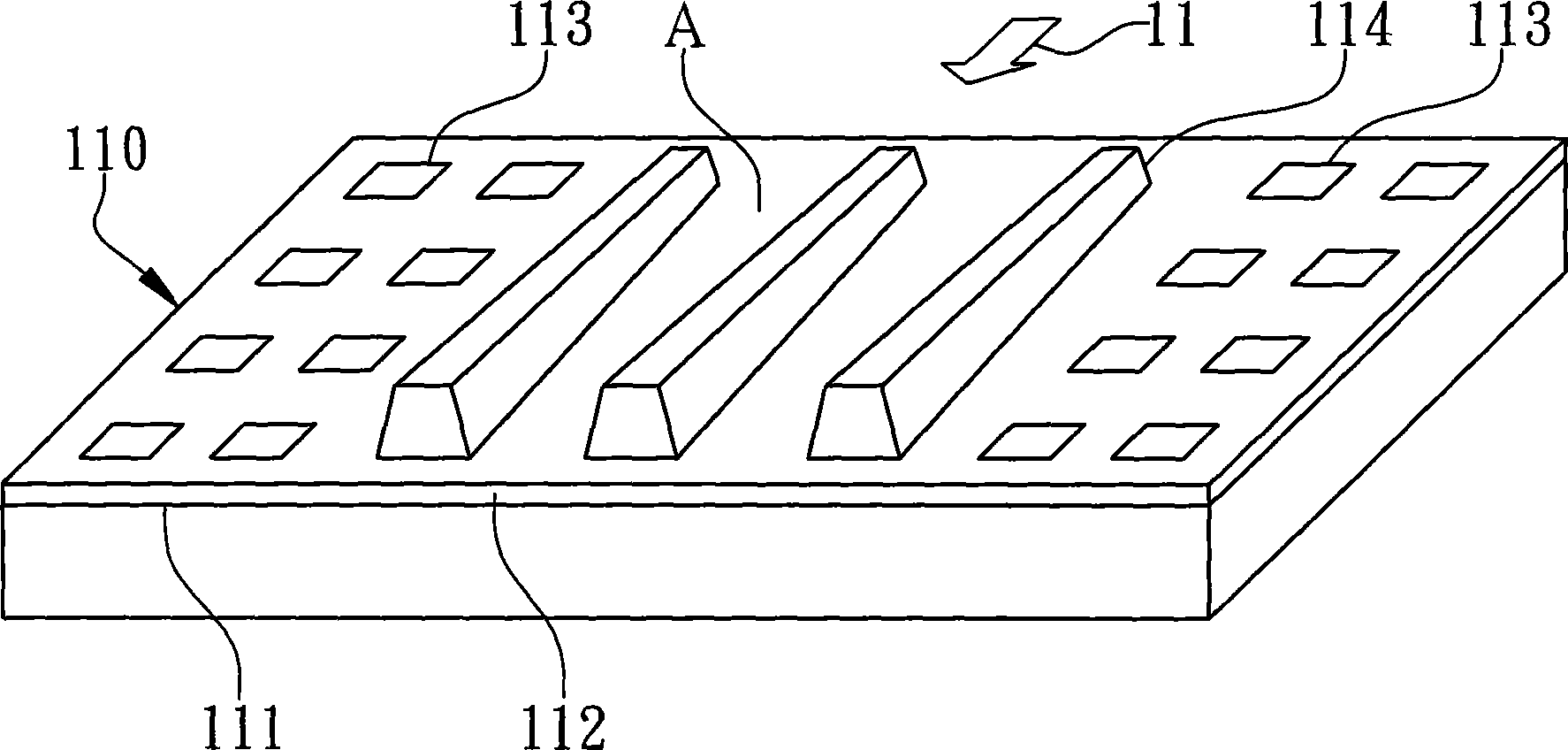
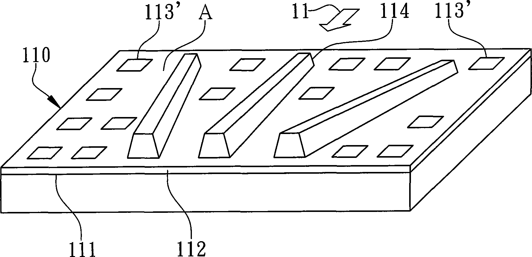
[0038] According to a specific embodiment of the present invention, a flip chip encapsulation structure of non-array bumps is illustrated in figure 1 The cross-sectional schematic diagram and figure 2 3D schematic diagram of the substrate. The flip chip encapsulation structure 100 of non-array bumps mainly includes a substrate 110, a chip 120 and a molding compound 130.

[0039] The substrate 110 has an upper surface 111 covered with a solder mask 112, and the upper surface 111 is provided with a plurality of pads 113 e...


PUM


Abstract

The invention relates to a flip chip molding structure and a flip chip molding method of a non-array bump. The flip chip molding structure of the non-array bump comprises a substrate, a chip and an epoxy molding compound, wherein the substrate is provided with an upper surface which is covered by an anti-welding layer, a plurality of connection cushions exposed out of the anti-welding layer and at least one mold flow conducting bar are arranged on the upper surface, and the mold flow conducting bar is arranged in a connection cushion-free blank area among the connection cushions, is higher than the connection cushions and the anti-welding layer and is protruded; the chip is provided with a plurality of bumps which are arranged in a non-array mode and are jointed onto the substrate in a flip chip mode, and a mold flow clearance is formed between the chip and the substrate; and the epoxy molding compound is formed on the upper surface of the substrate to seal a chip and is filled in the mold flow clearance. In the molding process, the mold flow conducting bar can guide mold flow and balance flow velocity, so that air bubbles or air holes are not generated in the mold flow clearance; and the flip chip molding structure and the flip chip molding method are particularly suitable for packaging a large number of metal post solder-chip connection frameworks in a molding manner.

Description

Technical field [0001] The invention belongs to the packaging structure and technical field of semiconductor devices, and in particular relates to a flip chip encapsulation structure and method for non-array bumps. Background technique [0002] At present, in the semiconductor industry, Flip Chip Package Technology is widely used in the field of chip packaging due to its many advantages such as reducing the packaging area and shortening the signal transmission path. In order to fully integrate the chip with the substrate, in the early days, an underfill was usually used to fill the gap between the chip and the substrate to overcome the stress caused by the difference in thermal expansion coefficient between the chip and the substrate, which caused the bumps to break and protect them. The interface between the chip and the substrate protects it from the environment (such as moisture). [0003] The conventional underfill glue uses a dispensing method on the side of the chip and uses...

Claims


Application Information

Patent Timeline
Patent Type & Authority Patents(China)
IPC IPC(8): H01L23/31H01L23/13H01L21/56
CPCH01L24/11H01L2224/11H01L2924/181H01L2924/00H01L2924/00012
Inventor 徐守谦柯志明徐宏欣
Owner POWERTECH TECHNOLOGY INC
Why Eureka
Try Eureka