Method for manufacturing semiconductor device

A semiconductor and device technology, applied in the field of semiconductor device manufacturing, can solve the adverse effects of semiconductor device threshold voltage control leakage and other characteristics, semiconductor device performance deviation from long channel characteristics, etc., to ensure reliability, reduce junction capacitance, Effect of reducing junction destabilization

Active Publication Date: 2012-10-17
SEMICON MFG INT (SHANGHAI) CORP
View PDF3 Cites 7 Cited by
  • Summary
  • Abstract
  • Description
  • Claims
  • Application Information

AI Technical Summary

Problems solved by technology

However, when the channel length is shortened to be comparable to the sum of the depletion layer widths of the source and drain, the perturbation caused by the channel edges (such as the source, drain, and insulating region edges) becomes more significant, The performance of semiconductor devices will deviate from the original long channel characteristics
For example, in short-channel conditions, the threshold voltage (i.e., the turn-on voltage of the gate) decreases as the drain voltage increases, which adversely affects the characteristics of semiconductor devices such as threshold voltage control and leakage

Method used


Image

  • Method for manufacturing semiconductor device
  • Method for manufacturing semiconductor device
  • Method for manufacturing semiconductor device

Examples


Embodiment Construction

[0029] In the following description, numerous specific details are given in order to provide a more thorough understanding of the present invention. It will be apparent, however, to one skilled in the art that the present invention may be practiced without one or more of these details. In other examples, some technical features known in the art are not described in order to avoid confusion with the present invention.

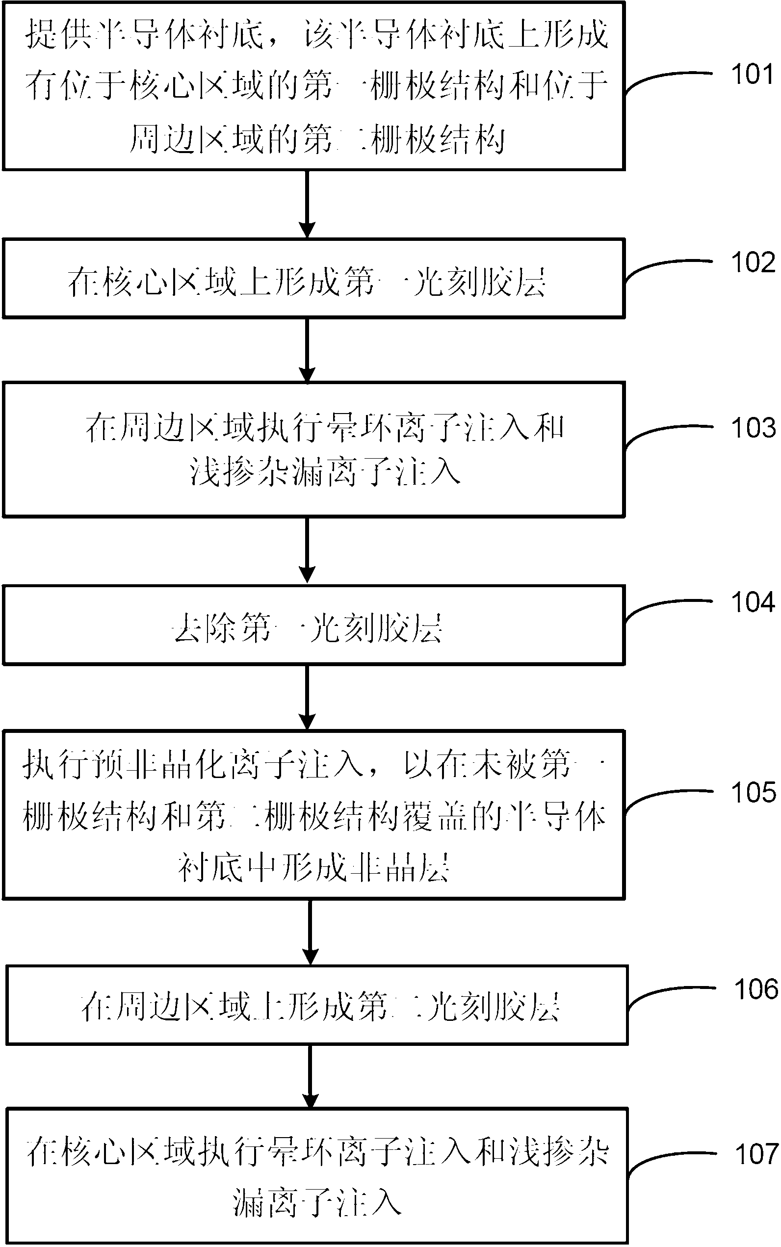
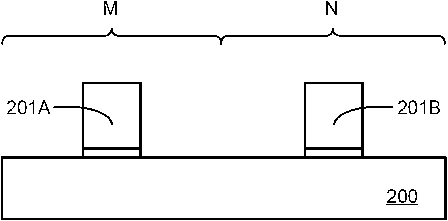
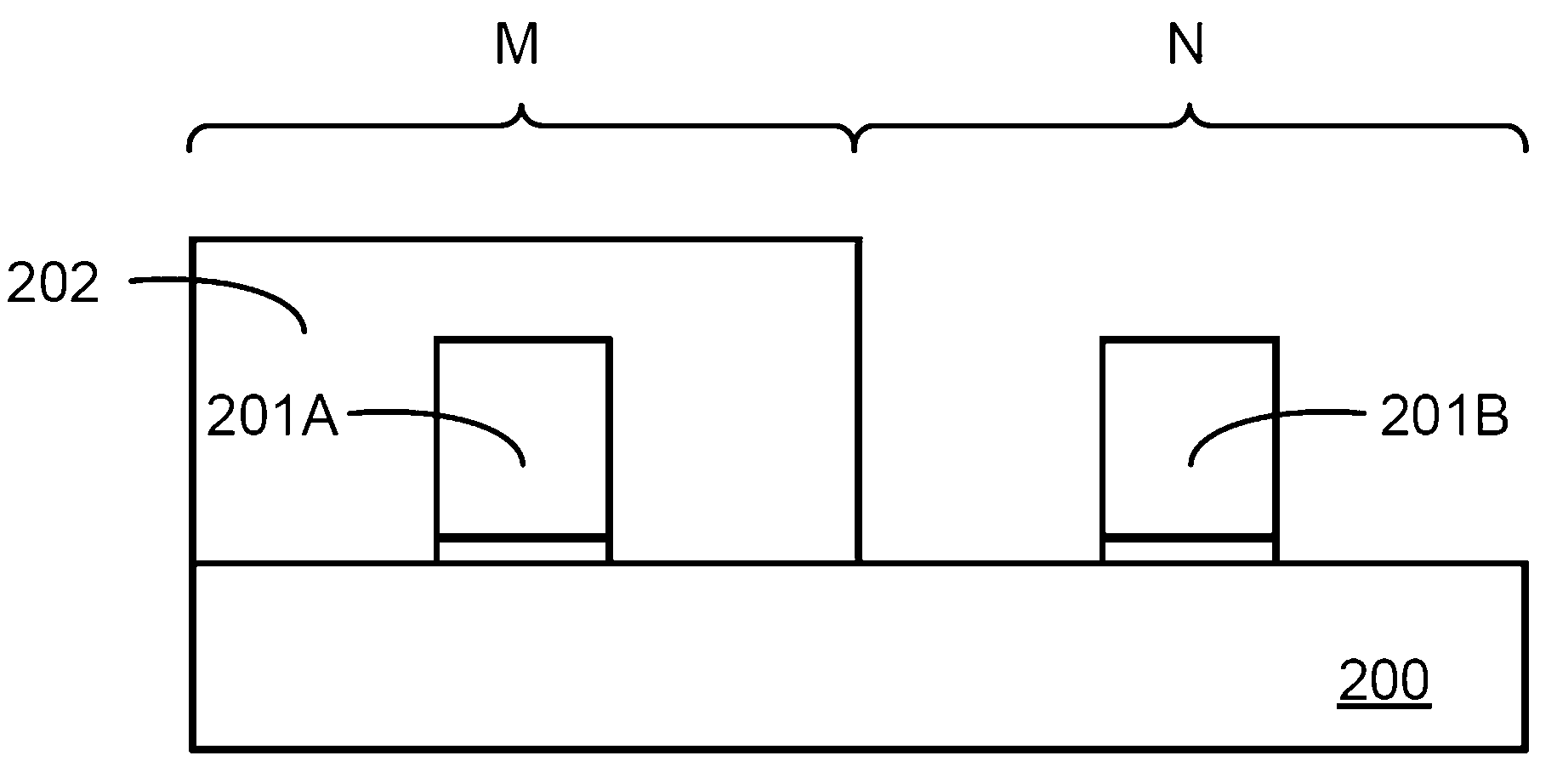
[0030] figure 1 It shows a process flow chart of manufacturing a semiconductor device according to an embodiment of the present invention, Figures 2A-2K A cross-sectional view of a device obtained by each step in the process flow of manufacturing a semiconductor device according to an embodiment of the present invention is shown. The following will combine figure 1 and Figures 2A-2K The manufacturing method of the present invention will be described in detail.

[0031] Step 101 is executed to provide a semiconductor substrate on which a first gate structu...


PUM


Abstract

The invention discloses a method for manufacturing a semiconductor device, comprising the steps of: providing a semiconductor substrate on which a first gate structure located in the core area and a second gate structure located in the peripheral area are formed; forming a first photoresist layer in the core area; performing pocket implantation and lightly doped drain implantation in the peripheral area to form a second pocket implantation region and a second lightly doped region in the semiconductor substrate on both sides of the second gate structure; removing the first photoresist layer; performing pre-amorphization implantation to form an amorphous layer in the semiconductor substrate not covered by the first gate structure and the second gate structure; forming a second photoresist layer in the peripheral area; and performing pocket implantation and lightly doped drain implantation in the core area to form a first pocket implantation region and a first lightly doped region in the semiconductor substrate on both sides of the first gate structure. The method of the invention can help reduce junction mutability and junction capacitance of the core area while ensuring reliability of hot electron injection of devices in the peripheral area.

Description

technical field [0001] The invention relates to a semiconductor manufacturing process, in particular to a method for manufacturing a semiconductor device. Background technique [0002] With the increasing demand for high integration and high performance of VLSI, the critical dimensions of semiconductor devices are getting smaller and smaller. However, when the channel length is shortened to be comparable to the sum of the depletion layer widths of the source and drain, the perturbation caused by the channel edges (such as the source, drain, and insulating region edges) becomes more significant, The performance of semiconductor devices will deviate from the original long channel characteristics. For example, in short-channel conditions, the threshold voltage (i.e., the turn-on voltage of the gate) decreases as the drain voltage increases, which adversely affects the threshold voltage control and leakage characteristics of semiconductor devices. The above-mentioned influence...

Claims


Application Information

Patent Timeline
Patent Type & Authority Applications(China)
IPC IPC(8): H01L21/336H01L21/28H01L21/265
Inventor 甘正浩
Owner SEMICON MFG INT (SHANGHAI) CORP
Why Eureka
Try Eureka