A Method for Improving the Reliability of Sonns Structured Devices Using Asymmetric Hierarchical Barriers

An asymmetric and reliable technology, applied in the field of microelectronics, can solve problems such as the reduction of the potential height and the influence of the charge retention ability, and achieve the effect of improving reliability.

Active Publication Date: 2015-09-30
SHANGHAI HUALI MICROELECTRONICS CORP
View PDF5 Cites 0 Cited by
  • Summary
  • Abstract
  • Description
  • Claims
  • Application Information

AI Technical Summary

Problems solved by technology

[0007] However, for silicon nitride with a smaller potential barrier, the charge retention ability will be affected to a certain extent, and the height of the potential barrier does not decrease when a voltage is applied, such as figure 2 As shown in , where, when the gate voltage V is added to the SONOS structure device, although the energy band after the voltage is added (such as figure 2 Shown by the dotted line in the middle) relative to the energy band when no voltage is applied (such as figure 2 (shown by the solid line in the center) has shifted, but the height of the potential has not decreased

Method used


Image

  • A Method for Improving the Reliability of Sonns Structured Devices Using Asymmetric Hierarchical Barriers
  • A Method for Improving the Reliability of Sonns Structured Devices Using Asymmetric Hierarchical Barriers
  • A Method for Improving the Reliability of Sonns Structured Devices Using Asymmetric Hierarchical Barriers

Examples


Embodiment Construction

[0033] The present invention will be further described below in combination with principle diagrams and specific operation examples.

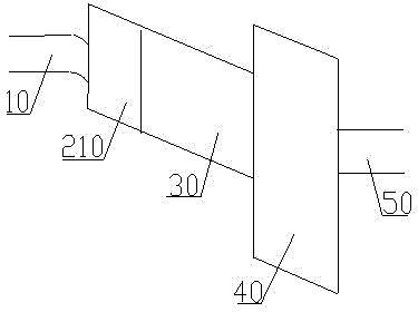
[0034] combine Figure 4 and Figure 5 Shown in, a method for improving the reliability of a SONNS structure device by using an asymmetric layered barrier, including the following steps:

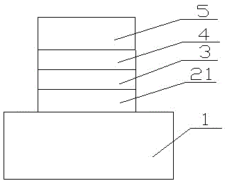
[0035] Step S1: providing a P-type substrate 1;

[0036] S2: forming a layer of tunneling silicon nitride layer 21 and a layer of tunneling oxide layer 22 of equal electrical thickness on the P-type substrate 1;

[0037] In one embodiment of the present invention, a layer of silicon nitride layer without charge trapping capability is formed on the P-type substrate 1, the thickness of the silicon nitride layer is 2-3nm, as the tunneling silicon nitride layer 21, In addition, a tunneling oxide layer 22 is formed on the tunneling silicon nitride layer 21, which together constitute a tunneling dielectric layer, and the tunneling oxide layer 22 has the same ele...


PUM

PropertyMeasurementUnit
thicknessaaaaaaaaaa
thicknessaaaaaaaaaa
thicknessaaaaaaaaaa

Abstract

The invention discloses a method for improving the reliability of a self organizing neural networks (SONNs) structure device by using an asymmetric layered potential barrier. The method comprises the following steps of: 1, providing a P-type substrate; 2, manufacturing a tunneling silicon nitride layer and a tunneling oxidation layer with equal electrical thickness; 3, manufacturing a memory silicon nitride layer on the surface of the tunneling oxidation layer; 4, manufacturing a blocking oxidation layer on the memory silicon nitride layer; and 5, manufacturing polycrystalline silicon on the blocking oxidation layer. The invention aims to provide the method for improving the reliability of the SONNs structure device by using the asymmetric layered potential barrier. The method is high in charge holding capacity, and a cavity in an erasure state can be prevented from entering an interface state in compiling and erasure cycles, so the durability of the device is improved.

Description

technical field [0001] The invention relates to the field of microelectronics, in particular to a method for improving the reliability of a SONNS structure device by using an asymmetric layered potential barrier. Background technique [0002] Flash memory is a type of non-volatile memory device. Traditional flash memory uses polysilicon floating gates to store data. Since polysilicon is a conductor, the charges stored in the floating gates are continuously distributed. When there is a leakage channel, the charge stored in the entire floating gate will be lost through this leakage channel. The recently developed SONOS structure replaces the original polysilicon charge storage layer with a silicon nitride layer capable of trapping charges. Since it uses trap energy levels to store charges, the stored charges are discretely distributed. Such a leakage channel will not cause a large leakage current, so the reliability is greatly improved. [0003] The SONOS structure has becom...

Claims


Application Information

Patent Timeline
Patent Type & Authority Patents(China)
IPC IPC(8): H01L27/115H01L21/8247
Inventor 田志
Owner SHANGHAI HUALI MICROELECTRONICS CORP
Why Eureka
Try Eureka