
Display device with built-in pixel compensation function, display panel and manufacturing method thereof

A technology for display panels and manufacturing methods, applied to static indicators, semiconductor/solid-state device components, instruments, etc., capable of solving the problems of light shading of electroluminescent elements, low aperture ratio of top-emitting OLED devices, photosensitive detection elements and their drives Circuit opacity and other problems, to ensure the detection accuracy, prevent the impact, improve the effect of aperture ratio

Active Publication Date: 2022-05-27
BOE TECH GRP CO LTD
View PDF0 Cites 0 Cited by
  • Summary
  • Abstract
  • Description
  • Claims
  • Application Information

AI Technical Summary

Problems solved by technology

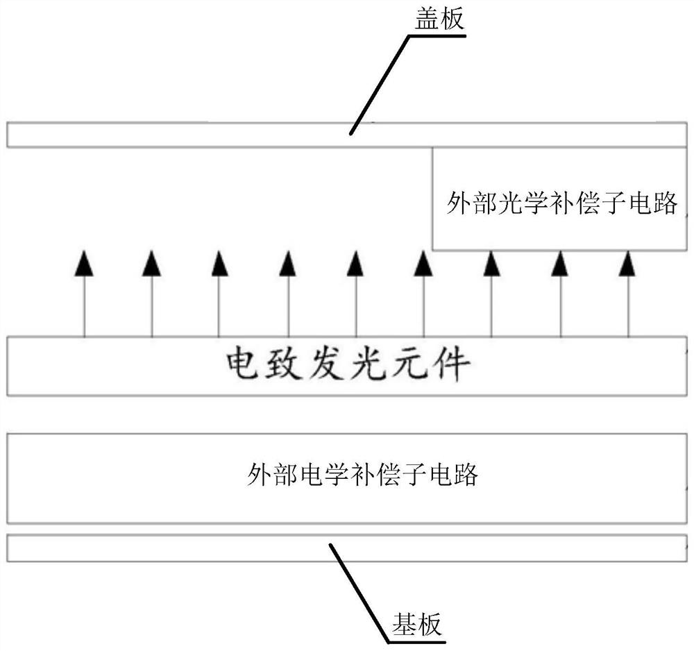
[0007] However, usually the cover plate of the display device is made of transparent material, such as glass, organic film, etc., so that the light of the electroluminescent element can pass through; however, the photosensitive detection element and its driving circuit are opaque; therefore, the The photosensitive detection element and its driving circuit in the external optical compensation sub-circuit will block the light of the electroluminescent element, resulting in a lower aperture ratio of the top-emitting OLED device, thereby affecting the display effect of the display device

Method used


Image

  • Display device with built-in pixel compensation function, display panel and manufacturing method thereof
  • Display device with built-in pixel compensation function, display panel and manufacturing method thereof
  • Display device with built-in pixel compensation function, display panel and manufacturing method thereof

Examples


Embodiment Construction

[0059] In order to make the objectives, technical solutions and advantages of the present invention clearer, the present invention will be further described in detail below with reference to specific embodiments and accompanying drawings.

[0060] The following describes in detail the embodiments of the present invention, examples of which are illustrated in the accompanying drawings, wherein the same or similar reference numerals refer to the same or similar elements or elements having the same or similar functions throughout. The embodiments described below with reference to the accompanying drawings are exemplary and are only used to explain the present invention, but not to be construed as a limitation of the present invention.

[0061] It will be understood by those skilled in the art that the singular forms "a", "an", "the" and "the" as used herein can include the plural forms as well, unless expressly stated otherwise. As used herein, the term "and / or" includes all or a...


PUM


Abstract

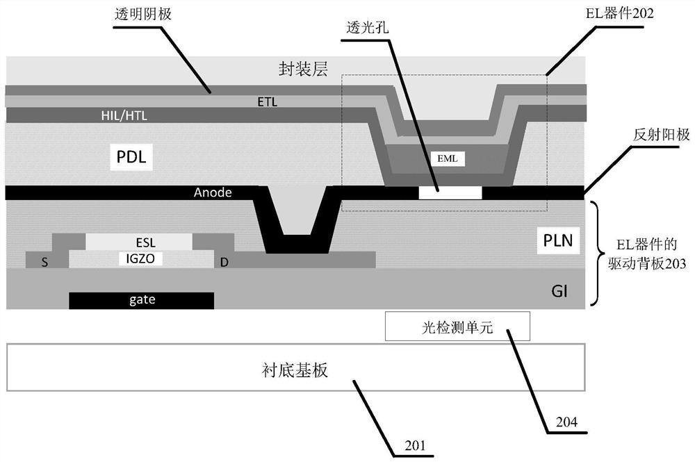
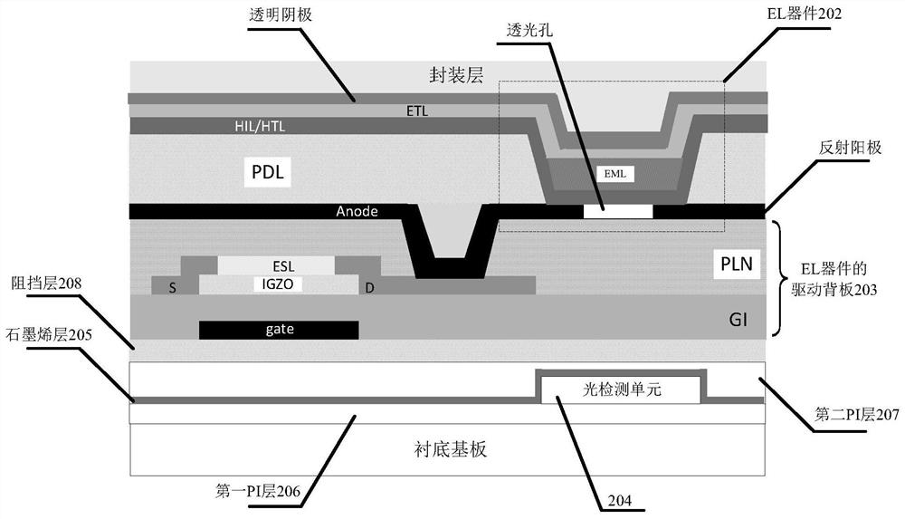
The invention discloses a display device with a built-in pixel compensation function, a display panel and a manufacturing method thereof. The display panel includes: a base substrate, an electroluminescent EL device, and an electroluminescent EL device arranged between the EL device and the base substrate. The driving backplane of the EL device, and the light detection unit arranged between the driving backplane and the base substrate; wherein, the reflective anode of the EL device is provided with a light-transmitting hole and the light detection unit The photosensitive detection elements in the unit are opposite; the photodetection unit is used to detect the brightness signal of the EL device through the light transmission hole, and output an electrical signal as the basis for pixel compensation of the EL device. The application of the present invention can perform real-time Demura compensation without blocking the light of the electroluminescent element, increases the aperture ratio of the top-emitting OLED device, and avoids affecting the display effect of the display device.

Description

technical field [0001] The present invention relates to the field of display technology, in particular to a display device with built-in pixel compensation function, a display panel and a manufacturing method thereof. Background technique [0002] OLED (Organic Light-Emitting Diode) or AMOLED (Active-matrix organic light-emitting diode), as a current-mode light-emitting device, has been increasingly used in high-performance Displaying. Due to its self-luminous characteristics, it has many advantages such as high contrast ratio, ultra-thin and light compared with LCD. However, brightness uniformity and afterimage are still the two main problems it is currently facing. To solve these two problems, in addition to process improvement, compensation technology has to be mentioned. Compensation methods can be divided into two categories: internal compensation and external compensation. Internal compensation refers to a method in which a sub-circuit constructed by a TFT (Thin Fil...

Claims


Application Information

Patent Timeline
Patent Type & Authority Patents(China)
IPC IPC(8): H01L27/32H01L23/367H01L23/373G09G3/3208
CPCH01L23/367G09G3/3208H01L23/373
Inventor 张永峰焦志强
Owner BOE TECH GRP CO LTD
Learn More