Method for restraining boron impurities expanding in P-shaped pseudo buried layer

A pseudo-buried layer and heavy doping technology, which is applied in semiconductor/solid-state device manufacturing, electrical components, circuits, etc., to ensure performance and suppress external expansion

Inactive Publication Date: 2013-04-10
SHANGHAI HUAHONG GRACE SEMICON MFG CORP
View PDF3 Cites 0 Cited by
  • Summary
  • Abstract
  • Description
  • Claims
  • Application Information

AI Technical Summary

Problems solved by technology

Since the implanted impurity in the P-type pseudo-buried layer is boron, the boron atoms will expand during the annealing process, such as figure 1 As shown in (b), the undoped or N-type lightly doped region 501 is doped with boron on the surface of the shallow trench to become a P-type region 201

Method used


Image

  • Method for restraining boron impurities expanding in P-shaped pseudo buried layer
  • Method for restraining boron impurities expanding in P-shaped pseudo buried layer

Examples


Embodiment Construction

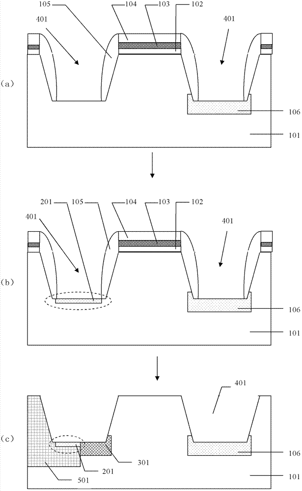
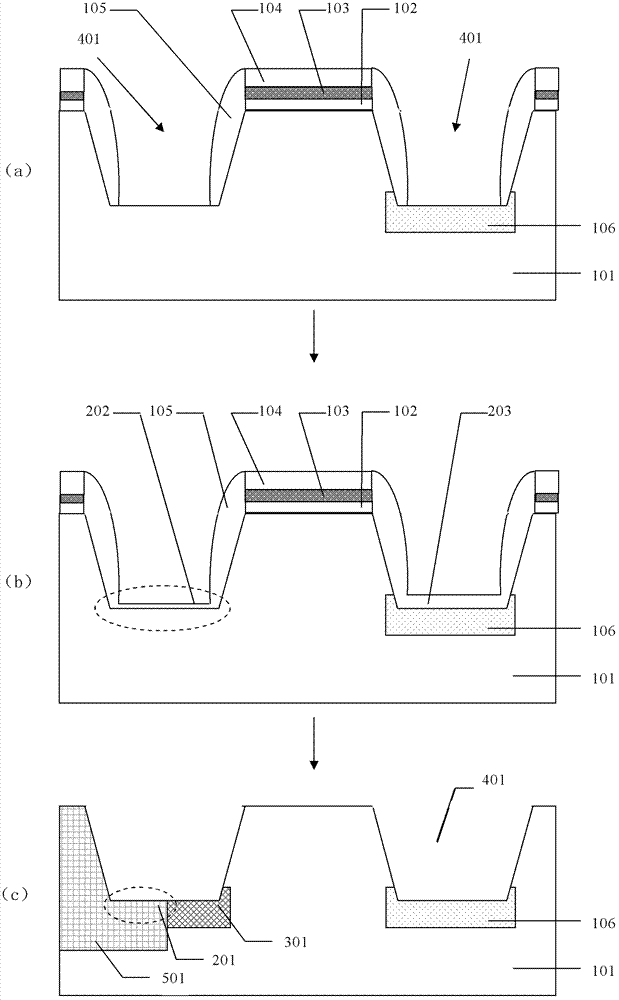
[0030] In order to have a more specific understanding of the technical content, characteristics and effects of the present invention, now in conjunction with the illustrated embodiment, the details are as follows:

[0031] In order to suppress the external expansion of boron impurities in the P-type pseudo-buried layer, the present invention improves the process flow of the SiGe BiCMOS pseudo-buried layer, and adopts the following process steps:

[0032] 1) Deposit silicon oxide 102 and silicon nitride 103 on the surface of the P-type silicon substrate 101; then use silicon nitride 103 as a barrier layer to etch a shallow trench isolation (STI) 401 structure; then make silicon oxide 104 and silicon oxide sidewalls 105 .

[0033] Wherein, the thickness of the silicon nitride 103 is 300˜1000 angstroms. The silicon oxide sidewall 105 has a thickness of 200-1200 angstroms.

[0034] 2) A high-concentration P-type impurity boron is implanted on the surface of the STI to form a hea...


PUM

PropertyMeasurementUnit
thicknessaaaaaaaaaa
thicknessaaaaaaaaaa

Abstract

The invention discloses a method for restraining boron impurities expanding in a P-shaped pseudo buried layer. The method includes the following steps: (1) depositing silicon oxide and silicon nitride on the surface of a silicon underlayer, then etching shallow trench separation structures on the P-shaped silicon underlayer with the silicon nitride as a barrier layer, subsequently forming the silicon nitride and a silicon nitride side wall, (2) injecting high concentration boron to form a heavy doping P-shaped pseudo buried layer, (3) annealing and boosting, and simultaneously carrying out mild oxidation, growing layers of the silicon nitride respectively on a P-shaped pseudo buried layer area and a non-heavy doping area, and then (4) infusing a heavy doping N-shaped pseudo buried layer. At the time of annealing and boosting, the mild oxidation is simultaneously carried out. A layer of thick silicon nitride grows on the silicon surface of the P-shaped pseudo buried layer area, and a layer of thin silicon nitride grows on the silicon surface of the non-heavy doping area, and therefore expansion of the boron impurities in the P-shaped pseudo buried layer is restrained, and meanwhile infusion of the subsequent N-shaped pseudo buried layer can not be affected.

Description

technical field [0001] The invention relates to the field of semiconductor integrated circuit manufacturing, in particular to a method for suppressing the external expansion of boron impurities in a P-type pseudo-buried layer. Background technique [0002] In the SiGe BiCMOS (SiGe Bipolar Complementary Metal Oxide Semiconductor) process of Shanghai Huahong NEC Electronics Co., Ltd., the original deep hole contact process and pseudo buried layer (Pseudo Buried Layer) are adopted, which can make The device has the characteristics of small area and low cost. Among them, the current process steps of the pseudo-buried layer process are: [0003] 1) Deposit silicon oxide 102 and silicon nitride 103 on the surface of the silicon substrate, and then use silicon nitride as a barrier layer to etch a shallow trench isolation (STI) 401 structure on the P-type silicon substrate, and then make silicon oxide 104 and silicon oxide sidewalls 105 . The silicon nitride 103 barrier layer has...

Claims


Application Information

Patent Timeline
Patent Type & Authority Applications(China)
IPC IPC(8): H01L21/762H01L21/265
CPCH01L21/26513H01L21/8249H01L21/265
Inventor 刘冬华段文婷石晶钱文生胡君
Owner SHANGHAI HUAHONG GRACE SEMICON MFG CORP
Why Eureka
Try Eureka