Electrical apparatus and manufacturing process of the same
一种电器装置、制造方法的技术,应用在的电器装置领域,能够解决熔敷面面积有限、难壳体半体合体强度等问题
- Summary
- Abstract
- Description
- Claims
- Application Information
AI Technical Summary
Problems solved by technology
Method used
Image
Examples
Embodiment Construction
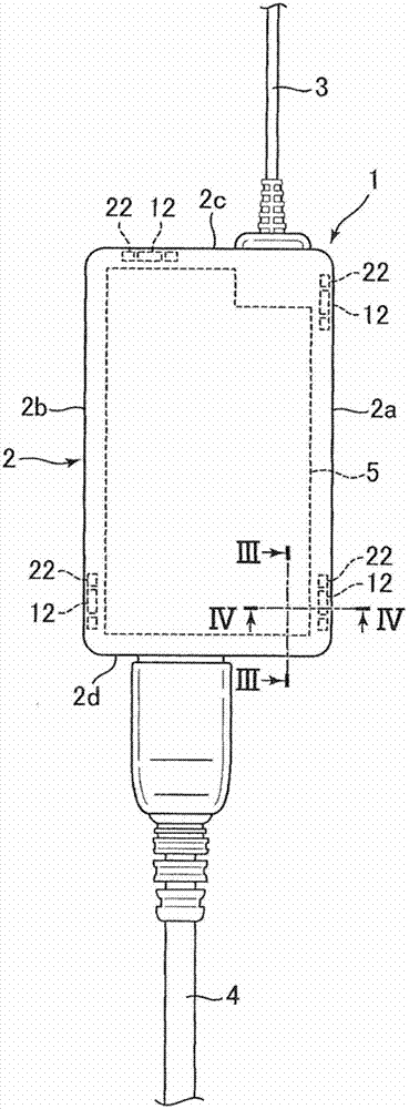
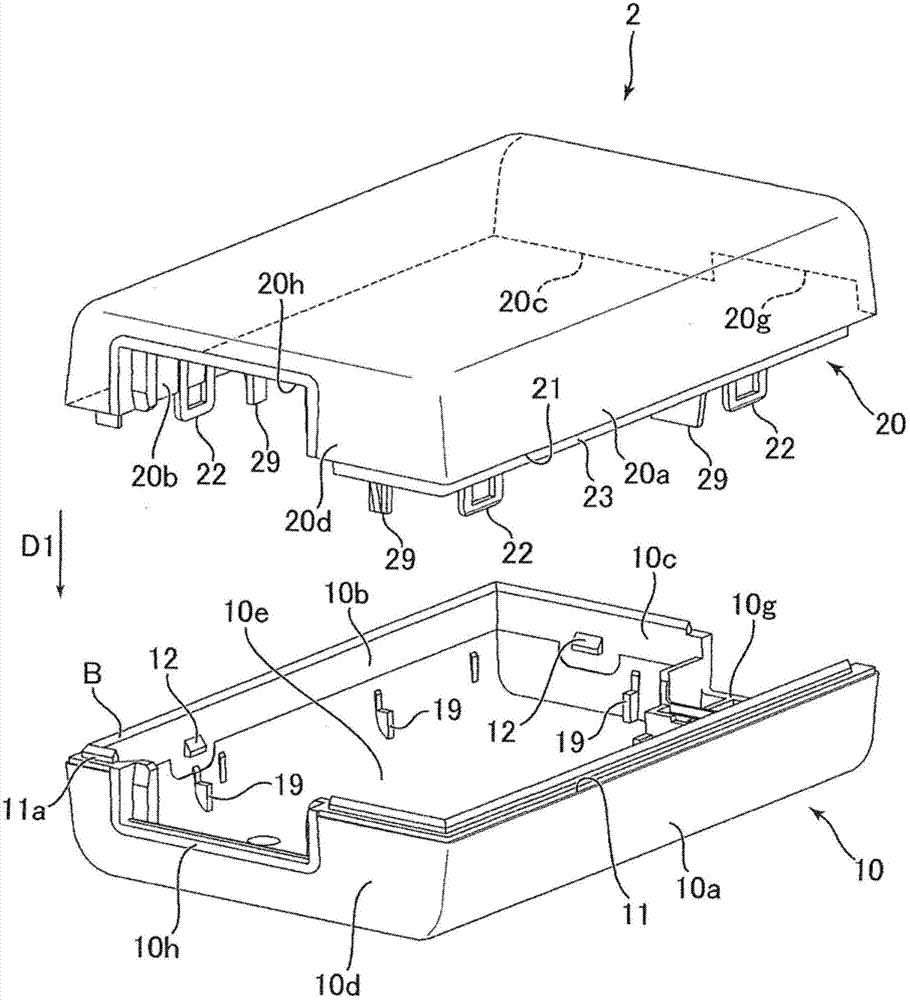
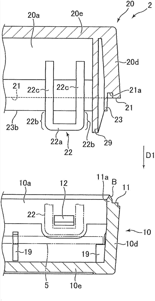
[0010] Below, while referring to the attached Figure 1 One embodiment of the present invention will be described. figure 1 It is a top view of the electrical device 1 according to the embodiment of the present invention. figure 2 It is an exploded perspective view of the case 2 included in the electric device 1 . image 3 It is to figure 1 The line III-III shown is a cross-sectional view of the casing 2 as a cutting plane. Figure 4 It is to figure 1 The IV-IV line shown is a cross-sectional view of the housing 2 as a cutting plane. figure 2 and image 3 The first casing half body 10 that represents the state before the first casing half body 10 and the second casing half body 20 that constitute the casing 1 are combined, shows that the first casing half body 10 and the second casing half body 20 Melted convex portion B that is melted during welding.
[0011] The electric device 1 of this example is connected to a portable electronic device such as a personal compute...
PUM
 Abstract
Description
Claims
Application Information


