Liquid crystal display panel and display device

A technology of liquid crystal display panels and thin film transistors, applied in static indicators, nonlinear optics, instruments, etc., can solve the problems of screen flickering, image interference, high power consumption, etc., and achieve the effect of low power consumption and clear pictures

Active Publication Date: 2016-01-13
TCL CHINA STAR OPTOELECTRONICS TECH CO LTD
View PDF5 Cites 0 Cited by
  • Summary
  • Abstract
  • Description
  • Claims
  • Application Information

AI Technical Summary

Problems solved by technology

[0007] An object of the present invention is to provide a liquid crystal display panel to solve the problem in the prior art that the displayed picture flickers, the images are disturbed, and the power consumption is relatively high due to the constant fluctuation of the common electrode voltage of the color filter substrate. question

Method used


Image

  • Liquid crystal display panel and display device
  • Liquid crystal display panel and display device
  • Liquid crystal display panel and display device

Examples


Embodiment Construction

[0031] The following descriptions of the various embodiments refer to the accompanying drawings to illustrate specific embodiments in which the present invention can be practiced. The directional terms mentioned in the present invention, such as "up", "down", "front", "back", "left", "right", "inside", "outside", "side", etc., are for reference only The orientation of the attached schema. Therefore, the directional terms used are used to illustrate and understand the present invention, but not to limit the present invention. In the figures, structurally similar units are denoted by the same reference numerals.

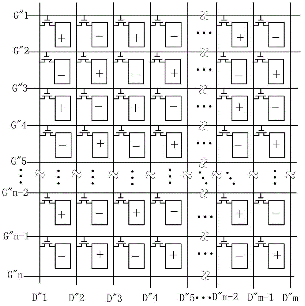
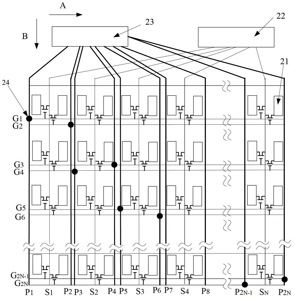
[0032] see figure 2 , figure 2 It is a schematic diagram of the pixel structure of a preferred embodiment of the liquid crystal display panel in the present invention. The liquid crystal display panel 20 includes a plurality of pixel matrices arranged along the row direction A and the column direction B. Each pixel matrix is ​​provided with a pixel unit 21 , a th...


PUM


Abstract

A liquid crystal display panel (20) and a display device are provided. An Nth row of scanning line groups is arranged between an Nth row and an N+1th row of pixel matrices of the liquid crystal display panel (20). Each row of scanning line groups comprises an upper scanning line (G2N-1) and a lower scanning line (G2N). The upper scanning line (G2N-1) and the lower scanning line (G2N) in each row of scanning line groups are alternatively connected with the gate electrodes of the thin film transistors of the adjacent columns of pixel matrices. An Nth column of data lines (SN) is arranged between a 2N-1th column of pixel matrices and a 2Nth column of pixel matrices. The Nth column of data lines (SN) is respectively connected with the source electrodes of the thin film transistors in the 2N-1th column of pixel matrices and the 2Nth column of pixel matrices adjacent to the Nth column of data lines (SN). By control of proper scanning sequence, the liquid crystal display panel (20) can realize dot inversion so as to obtain the effect of low power consumption and clear image, and can not be affected by uninterrupted changes of the voltage of the common electrode of the color filter substrate.

Description

【Technical field】 [0001] The invention relates to the technical field of liquid crystal display, in particular to a liquid crystal display panel and a display device. 【Background technique】 [0002] In recent years, liquid crystal displays have gradually become mainstream displays due to their light, thin, and small features. Various electronic devices currently on the market, such as mobile phones, personal digital assistants, digital cameras, computer screens, notebook computer screens, etc., almost all use liquid crystal display screens as their display screens. [0003] see figure 1 , figure 1 It is a schematic diagram of a pixel structure of a liquid crystal display panel in the prior art. The above-mentioned liquid crystal display panel includes m data lines D"1~D"m, n scanning lines G"1~G"n, the data lines and the scanning lines are arranged to cross each other, and the two adjacent data lines are adjacent to each other The intersecting area of ​​the two scan line...

Claims


Application Information

Patent Timeline
Patent Type & Authority Patents(China)
IPC IPC(8): G02F1/1362G02F1/133G09G3/36
CPCG09G3/3614G09G2300/0426G09G2310/0281
Inventor 赵国丁涛刘明
Owner TCL CHINA STAR OPTOELECTRONICS TECH CO LTD
Why Eureka
Try Eureka