Array substrate wiring structure, liquid crystal display panel and liquid crystal display

A liquid crystal display panel, wiring structure technology, applied in static indicators, instruments, nonlinear optics, etc., can solve the problems of frequently changing data lines, increasing the driving power consumption of driving integrated chips, etc.

Active Publication Date: 2019-05-28
WUHAN CHINA STAR OPTOELECTRONICS TECH CO LTD
View PDF5 Cites 0 Cited by
  • Summary
  • Abstract
  • Description
  • Claims
  • Application Information

AI Technical Summary

Problems solved by technology

Although this can improve the picture display quality, the driving integrated chip will frequently change the polarity of the data line output, thus greatly increasing the driving power consumption of the driving integrated chip.

Method used


Image

  • Array substrate wiring structure, liquid crystal display panel and liquid crystal display
  • Array substrate wiring structure, liquid crystal display panel and liquid crystal display
  • Array substrate wiring structure, liquid crystal display panel and liquid crystal display

Examples


Embodiment Construction

[0034] The following will clearly and completely describe the technical solutions in the embodiments of the present invention with reference to the accompanying drawings in the embodiments of the present invention. Obviously, the described embodiments are only some, not all, embodiments of the present invention. Based on the embodiments of the present invention, all other embodiments obtained by persons of ordinary skill in the art without making creative efforts belong to the protection scope of the present invention.

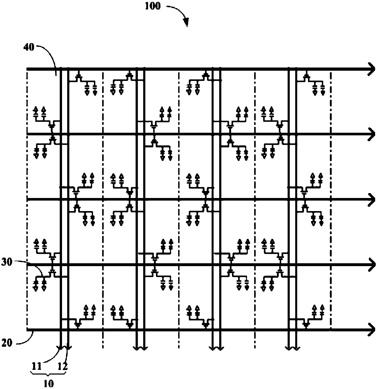
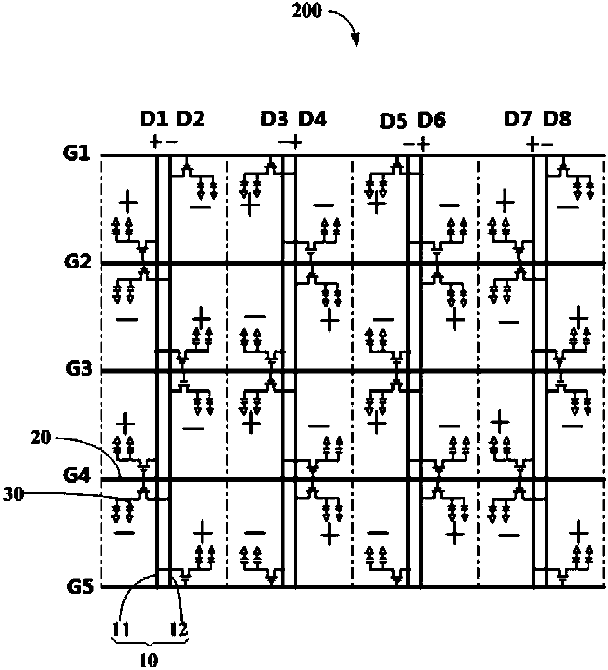
[0035] see figure 1 and figure 2 , the embodiment of the first solution of the present invention provides an array substrate wiring structure 100 . The array substrate wiring structure 100 is applied in a liquid crystal display panel. The array substrate wiring structure 100 includes several wiring units 200, and the several wiring units 200 are arranged sequentially from left to right and from top to bottom. Wherein, each wiring unit 200 includes first to...


PUM


Abstract

The invention provides an array substrate wiring structure. The wiring structure comprises a plurality of wiring units, each wiring unit comprises a first data line, a second data line, a third data line, a fourth data line, a fifth data line, a sixth data line, a seventh data line, an eighth data line, a first gate line, a second gate line, a third gate line, a fourth gate line, a fifth gate line and a thin film transistor matrix; the first data line, the fourth data line, the sixth data line and the seventh data line are taken as first data lines, the second data line, the third data line, the fifth data line and the eighth data line are taken as second data lines, the polarity of the first data lines is opposite to that of the second data lines, the first data lines are connected with source electrodes of thin film transistors in odd-numbered rows and odd-numbered columns and thin film transistors in even-numbered rows and even-numbered columns in a corresponding array, and the second data lines are connected with source electrodes of thin film transistors in odd-numbered rows and even-numbered columns and thin film transistors in even-numbered rows and odd-numbered columns in a corresponding array; the second gate line and the fourth gate line are connected with gate electrodes of two thin film transistors which are located in two adjacent rows of the first data line side, and the first gate line, the third gate line and the fifth gate line are connected with gate electrodes of two thin film transistors which are located in two adjacent rows of the second data line side, so that the polarity of each pixel in the pixel matrix corresponding to the thin film transistor matrix is opposite to that of any adjacent pixels.

Description

technical field [0001] The invention relates to the display field, in particular to an array substrate wiring structure, a display panel and a liquid crystal display. Background technique [0002] In the traditional red, green, blue, and white four-color LTPS (Low Temperature Poly-silicon, low temperature polysilicon technology) display technology, in order to reduce the number of tube corners and fan-out wiring at the drive integrated chip, a splitter is often designed to connect a The root trace is divided into 4 data lines, and the pixel data lines are determined by timing. But this will cause the polarity of the adjacent four data lines under the control of any fan-out line to be exactly the same, and the liquid crystal realizes a 4-column inversion mode during the polarity inversion process, which will greatly reduce the picture display quality . Usually, the data line crossover line of the control line in the adjacent fan is used to improve the limit inversion mode o...

Claims


Application Information

Patent Timeline
Patent Type & Authority Patents(China)
IPC IPC(8): G02F1/1362G02F1/1368G09G3/36
CPCG02F1/136286G02F1/1368G09G3/3648
Inventor 王聪
Owner WUHAN CHINA STAR OPTOELECTRONICS TECH CO LTD
Why Eureka
Try Eureka