Component transfer device and method

A technology for transferring devices and components, which is applied in the direction of electrical components, semiconductor/solid-state device manufacturing, circuits, etc.

Inactive Publication Date: 2015-07-22
PIONEER FA +1
View PDF5 Cites 0 Cited by
  • Summary
  • Abstract
  • Description
  • Claims
  • Application Information

AI Technical Summary

Problems solved by technology

[0003] However, the above-mentioned chip components are produced in a very large number from one wafer, so the component transfer device for transferring chip components is required to transfer a large number of chips in a short time.

Method used


Image

  • Component transfer device and method
  • Component transfer device and method
  • Component transfer device and method

Examples


Embodiment

[0077] Hereinafter, embodiments of the present invention will be described with reference to the drawings.

[0078] (1) Basic structure

[0079] The structure of the transfer apparatus 1 which is an embodiment of the component transfer apparatus of this invention is demonstrated, referring drawings.

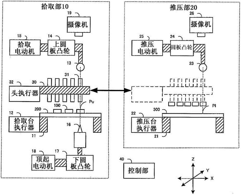
[0080] figure 1 It is a schematic diagram which shows the structure of the transfer apparatus 1. in the figure 1 In the following description, the left-right direction is defined as the X direction, the direction from the front side toward the depth measurement is defined as the Y direction, and the up-and-down direction is defined as the Z direction.

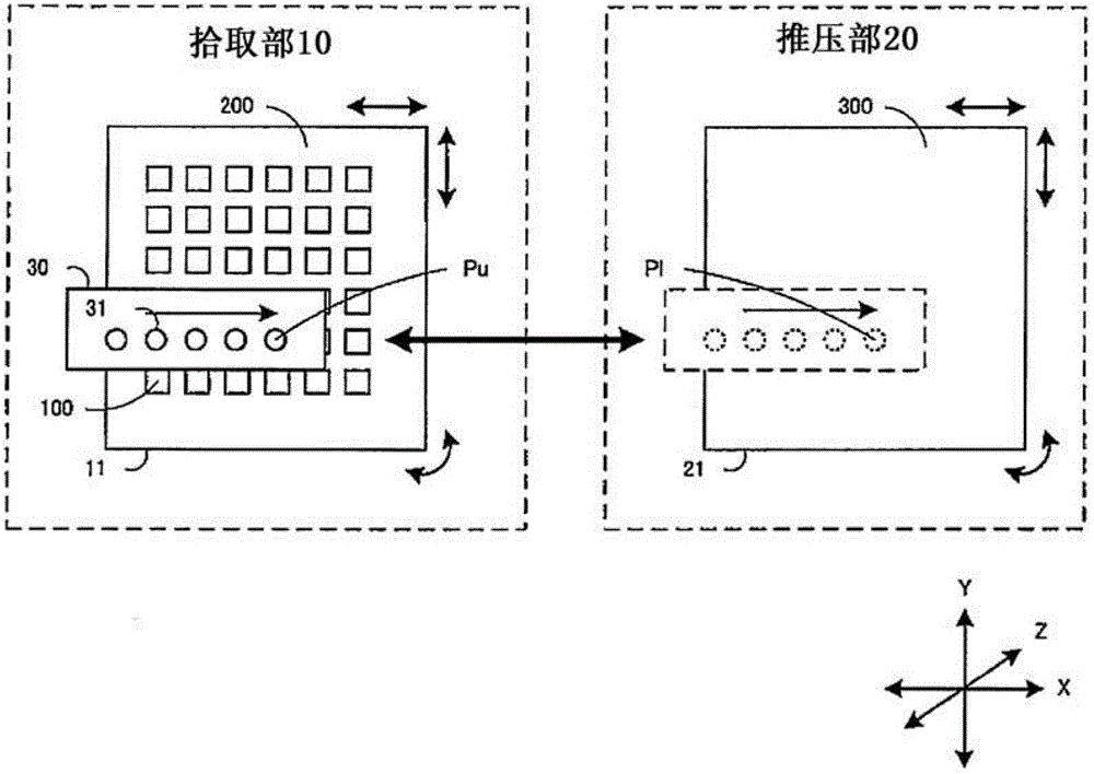
[0081] like figure 1 As shown, the transfer device 1 includes a pick-up unit 10 , a pressing unit 20 , a transfer head 30 and a control unit 40 . The pickup unit 10 and the pressing unit 20 are spaced apart from each other along the X direction.

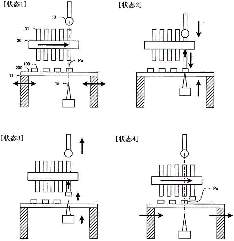
[0082] The pickup unit 10 is a unit for picking up the chip 100 from the adhes...


PUM


Abstract

A component transfer device (1) takes out wafer-shaped chips (100), which are held in holding units (11, 200), by means of suction nozzles (31). Acquisition means (19, 40) acquire position information about the chips in the holding units, and then, before a first chip from among the plurality of chips is adhered, position information about that first chip is re-acquired and thus updated. A determination means (40) (i) determines a movement amount for moving the first chip to a pick-up position, on the basis of the updated position information for the first chip, and (ii) determines a movement amount for moving chips other than the first chip to a pick-up position on the basis of revised position information, which is the position information for chips other than the first chip which are held in a specified region, using the first chip as a reference, in the holding unit, having been revised on the basis of the pre-update position information and post-update position information for the first chip. Movement means (12, 40) move the chips to the pickup position on the basis of the determined movement amounts.

Description

technical field [0001] The present invention relates to the technical field of a component transfer device that picks up electronic components such as chips and arranges them to a transfer destination. Background technique [0002] As such an apparatus, there is known an apparatus that picks up wafer-shaped chip components divided by dicing and arranges them to transfer destinations in each arrangement order. A conventional component transfer device picks up and transfers chips one by one by picking up chips from the upper side with a suction nozzle connected to a vacuum pump and pushing them up from the lower side. [0003] However, since the above-mentioned chip components are produced in a very large number from one wafer, a component transfer device for transferring chip components is required to transfer a large number of chips in a short time. For example, in order to shorten the tact time of the transfer process, a structure capable of transferring a plurality of chi...

Claims


Application Information

Patent Timeline
Patent Type & Authority Patents(China)
IPC IPC(8): H01L21/67H01L21/52
CPCH01L21/6838H01L21/68H01L21/67144
Inventor 藤森昭一清水寿治青木秀宪
Owner PIONEER FA
Why Eureka
Try Eureka