Backlight module and display device thereof

A technology of a backlight module and a light-transmitting layer, which is applied to lighting devices, non-electric lighting devices, fixed lighting devices, etc., can solve the problems affecting the display effect of the optical quality display device of the backlight module, etc., so as to improve the optical quality and reduce assembly. Cost, the effect of simplifying the assembly process

Active Publication Date: 2013-02-27
TCL CHINA STAR OPTOELECTRONICS TECH CO LTD
View PDF8 Cites 4 Cited by
  • Summary
  • Abstract
  • Description
  • Claims
  • Application Information

AI Technical Summary

Problems solved by technology

like figure 1 Shown is a schematic diagram of a side-entry LED backlight source of a backlight module in a liquid crystal display device, which includes the LED light bar 10 and the display area (that is, AA area) of the liquid crystal display device, and the value A is the length from the LED lamp to the AA area , P is the distance between two adjacent LED lamps, usually the ratio of A / P is greater than 0.5, but in the LED backlight side-type backlight module, with the narrow frame of the backlight module, the backlight The A value of the module is getting smaller and smaller. If the A / P ratio is less than 0.5, the Hotspot (firefly) phenomenon will easily occur, which seriously affects the optical taste of the backlight module and the display effect of the display device.

Method used


Image

  • Backlight module and display device thereof
  • Backlight module and display device thereof
  • Backlight module and display device thereof

Examples


Embodiment Construction

[0022] In order to better illustrate the technical means adopted by the present invention and its effects, a detailed description will be given below in conjunction with the embodiments of the present invention and the accompanying drawings, wherein the same reference numerals always represent the same components.

[0023] Such as Figure 5 Shown is a schematic structural view of a display device according to an embodiment of the present invention. The display device 400 includes an outer frame 100, a display panel 200, and a backlight module 300; The plastic frame 50 is fixed on the top of the backlight module 300 by components such as the outer frame 100 and the plastic frame 50 .

[0024] Hereinafter, the backlight module used in the display device of the embodiment of the present invention will be described in detail.

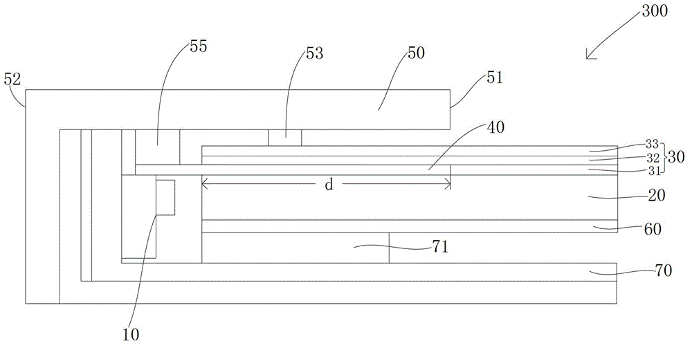
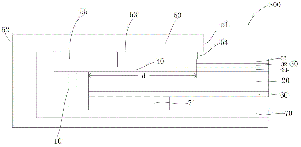
[0025] Such as figure 2 , image 3 Shown is the backlight module of the display device according to the present invention, the backlight module 300 inc...


PUM


Abstract

The invention discloses a backlight module and a display device thereof. The backlight module comprises a light guide board, a rubber frame and a plurality of point light sources which are adjacent to an input surface of the light guide board; the backlight module further comprises a non-light-transmitting layer; part of the non-light-transmitting layer is stuck on the rubber frame and the other part of the non-light-transmitting layer is arranged on an output surface of the light guide board; and the non-light-transmitting layer is used for shielding and absorbing part of light which is directly sent by a plurality of the point light sources, and light emitted by the output surface covered by the non-light-transmitting layer. With the adoption of the structure, an edge frame of the backlight module is narrowed; even if an A / P specific value is less than 0.5, a Host spot phenomenon can be avoided, so that the optical taste of the backlight module and the display effect of the display device are improved, an assembling process is simplified and the assembling cost is reduced.

Description

technical field [0001] The invention belongs to the field of liquid crystal display, and more specifically relates to a backlight module and a display device thereof. Background technique [0002] In the liquid crystal display device, the backlight module is one of the key components of the liquid crystal display device, which is mainly used to provide sufficient brightness and uniformly distributed light source so that the liquid crystal panel can display images normally. [0003] Generally, the LED backlight source in the backlight module can be divided into direct-input type directly under the light guide plate and side-input type by the side of the light guide plate. Such as figure 1 Shown is a schematic diagram of a side-entry LED backlight source of a backlight module in a liquid crystal display device, which includes the LED light bar 10 and the display area (that is, AA area) of the liquid crystal display device, and the value A is the length from the LED lamp to th...

Claims


Application Information

Patent Timeline
Patent Type & Authority Applications(China)
IPC IPC(8): F21S8/00F21V1/00G02F1/13357F21Y101/02
CPCF21V1/00G02F1/133308G02F1/133615G02B6/005G02B6/0088G02F1/133317G02B6/0035G02B6/0051G02B6/0053G02B6/0068G02B6/0073
Inventor 张光耀熊充
Owner TCL CHINA STAR OPTOELECTRONICS TECH CO LTD
Why Eureka
Try Eureka