Curved surface display panel

A curved surface display and panel technology, applied in nonlinear optics, instruments, optics, etc., can solve the problems of large relative movement, unevenness, and degradation of display quality between the light-shielding part and the pixel electrode, and achieve the effect of improving optical taste

Inactive Publication Date: 2019-09-24
WUHAN CHINA STAR OPTOELECTRONICS TECH CO LTD
View PDF5 Cites 5 Cited by
  • Summary
  • Abstract
  • Description
  • Claims
  • Application Information

AI Technical Summary

Problems solved by technology

[0004] The present invention provides a curved display panel to solve the problem of large relative movement between the light-shielding part and the pixel electrode during the bending process of the curved liquid crystal panel, so that color shift, dark state light leakage and The technical problem that the display quality is degraded due to bad phenomena such as uneven brightness

Method used


Image

  • Curved surface display panel
  • Curved surface display panel
  • Curved surface display panel

Examples


Embodiment 1

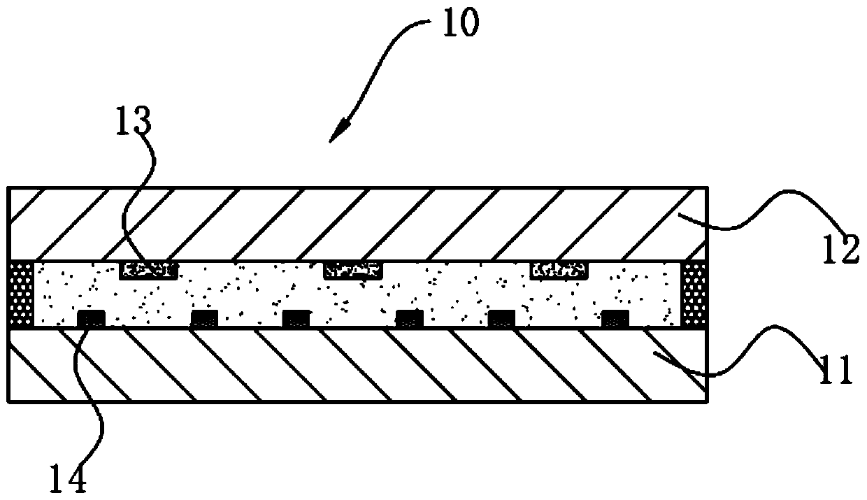
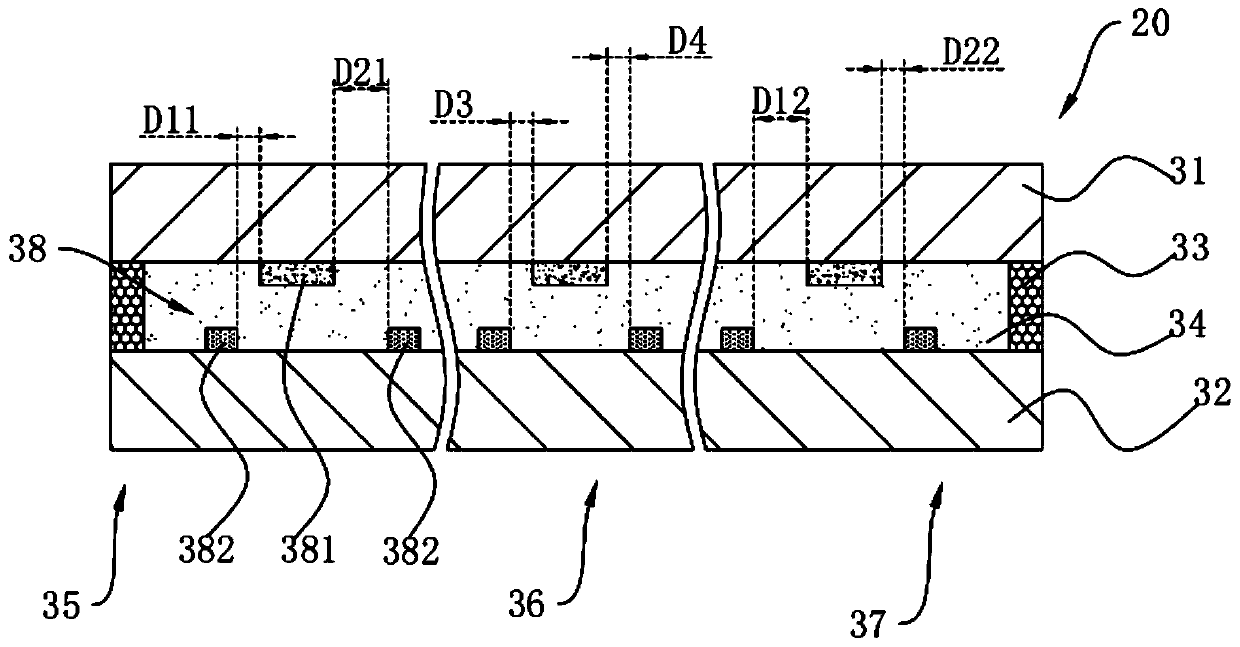
[0034] A curved display panel such as image 3 and Figure 4 As shown, the curved display panel 30 is formed by bending the flat display panel 20; the curved display panel 30 includes a curved color filter substrate 32, a curved surface array substrate 31, and The liquid crystal layer 34 on the 31 and the sealant 33; the sealant 33, the curved color filter substrate 32 and the curved array substrate 31 directly form an accommodating chamber for accommodating the liquid crystal layer 34.

[0035] Specifically, the side of the curved color filter substrate 32 away from the curved array substrate 31 is the light emitting surface of the curved display panel 30 , and the light emitting surface of the curved display panel 30 is a concave surface.

[0036] Specifically, a black matrix and a plurality of sub-pixels arranged at intervals are arranged between the curved surface array substrate 31 and the curved color filter substrate 32, and the black matrix includes light-shielding el...

Embodiment 2

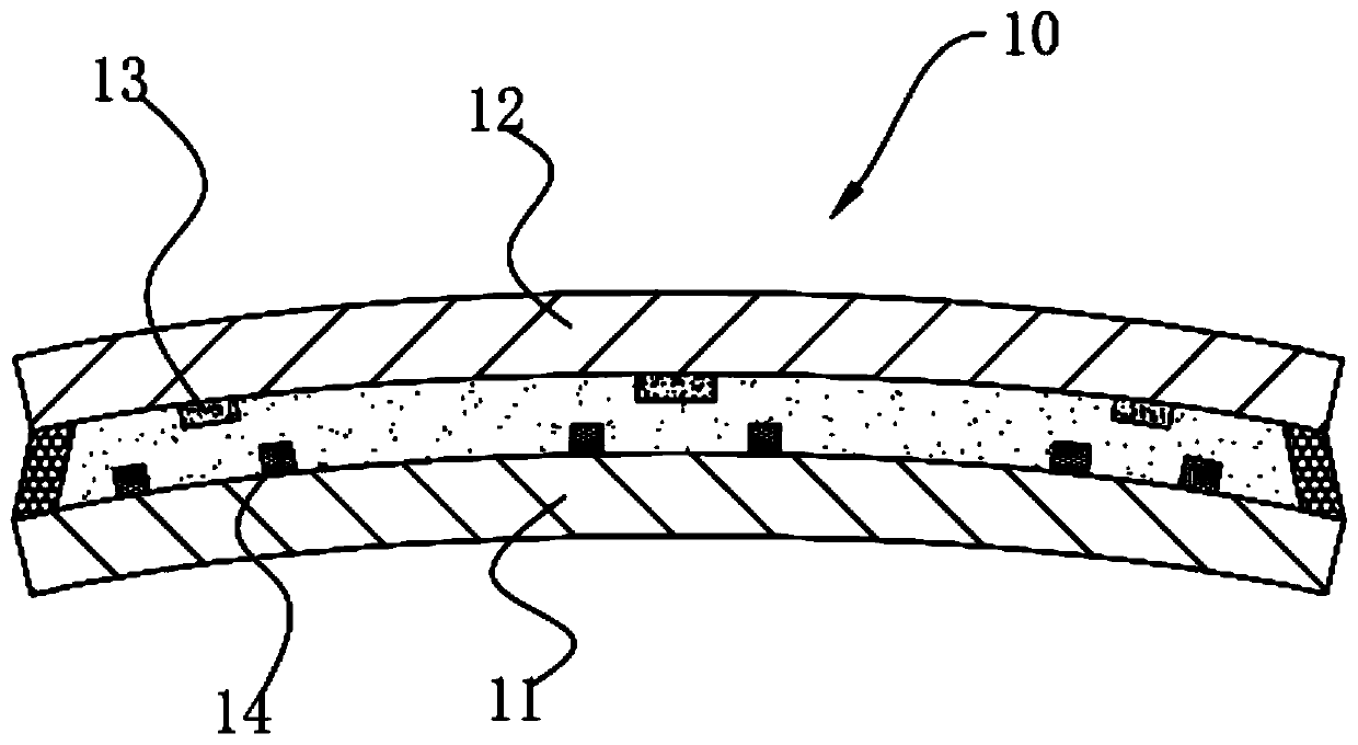
[0062] A curved display panel such as Figure 7 and Figure 8 As shown, the difference from Embodiment 1 is that the display surface of the curved display panel 30 is convex.

[0063] Specifically, when the curved display panel 30 is in a flattened state, D21 is smaller than D11, and D12 is smaller than D22.

[0064] It should be noted that those skilled in the art know that when the light-emitting surface of the curved display panel 30 is convex, during the process of bending the flat display panel 20 into the curved display panel 30, the left end of the curved array substrate 31 moves relatively to the left, and the right end Relatively move to the right; when the curved display panel 30 is in a flattened state, D21 is set to be smaller than D11, and D12 is smaller than D22. When the flat display panel 20 is bent into a curved display panel 30, displacement compensation is used to make D21 equal to or D11 is approximately equal to D12, and D12 is equal to or approximately ...


PUM


Abstract

The invention provides a curved surface display panel. The curved surface display panel comprises a curved-surface color film substrate, a curved-surface array substrate, and a liquid crystal layer. The curved surface display panel includes a plurality of pixel modules, each of the pixel modules includes a pixel electrode and two shading blocks which are located on two sides of the pixel electrode and adjacent to the pixel electrode. The curved surface display panel comprises a central section area and lateral areas located on two sides of the central section area. In each pixel module at the lateral areas of the curved surface display panel, distances between a front projection of the pixel electrode on the curved surface color film substrate and the two shading blocks is D1 and D2. When the curved surface display panel is in a flattening state, the D1 and the D2 are not equal. And when the curved surface display panel is in a curved state, the D1 is equal to the D2.

Description

technical field [0001] The invention relates to the field of display technology, in particular to a curved display panel. Background technique [0002] The curved LCD panel is the core component of the curved LCD. Such as figure 1 As shown, the existing curved liquid crystal panel 10 generally includes a color filter (CF) substrate 11 and a thin film silicon transistor (TFT) substrate 12 oppositely arranged, and the pixel electrodes 13 arranged at intervals are arranged on the TFT substrate 12, and the CF A black matrix formed of a black color resist material is provided on the substrate 11. The black matrix includes a plurality of light-shielding parts 14 arranged at intervals. The positions of the light-shielding parts 14 and the pixel electrodes 13 are arranged alternately. , the distance between the light shielding portion 14 and the corresponding pixel electrode 13 is a set value. [0003] However, if figure 2 As shown, when the curved liquid crystal panel 10 is in...

Claims


Application Information

Patent Timeline
Patent Type & Authority Applications(China)
IPC IPC(8): G02F1/1335
CPCG02F1/133512
Inventor 李雪云唐岳军
Owner WUHAN CHINA STAR OPTOELECTRONICS TECH CO LTD
Why Eureka
Try Eureka