Display apparatus and image pickup apparatus
一种显示装置、发光层的技术,应用在有机半导体器件、电固体器件、半导体器件等方向,能够解决金属掩模制备和维护困难等问题
- Summary
- Abstract
- Description
- Claims
- Application Information
AI Technical Summary
Problems solved by technology
Method used
Image
Examples
Embodiment
[0060] Embodiments according to aspects of the present invention are described below. Materials and element configurations used in the embodiments are just examples and the present invention is not limited to them.
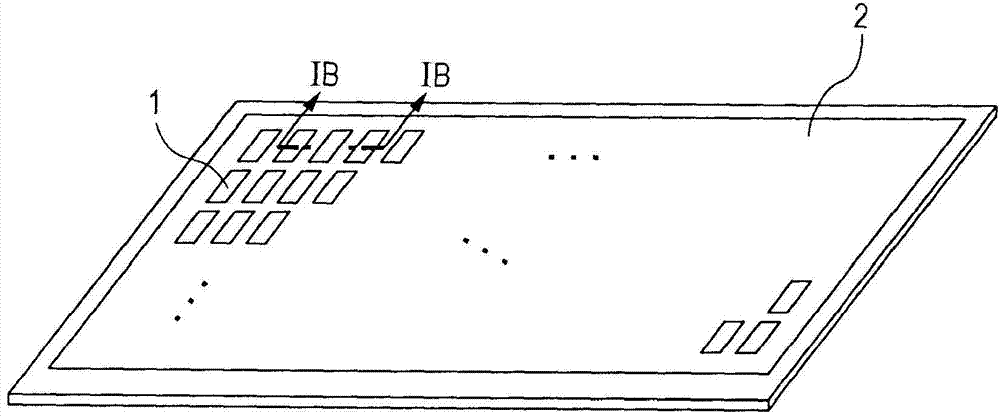
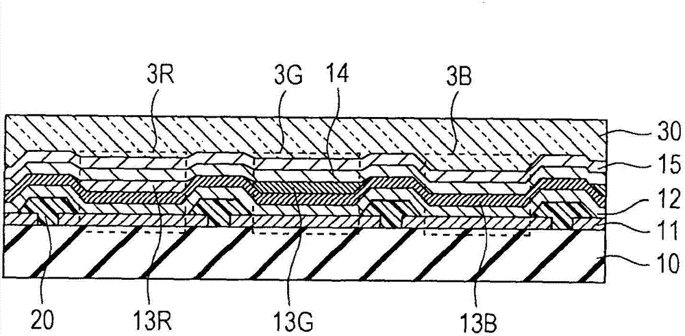
[0061] A display device is prepared, which has Figure 1B The configuration shown in , in addition, there is a configuration in which an electron injection layer is provided between the electron transport layer 14 and the cathode 15 .
[0062] A pixel circuit is formed on a glass substrate by low-temperature polysilicon TFTs. An interlayer insulating film made of SiN and a planarizing film made of acrylic resin are sequentially formed thereon so that Figure 1B Substrate 10 shown in . Anode 11 was formed by laminating silver (film thickness 200 nm) serving as a metal film and IZO (film thickness 20 nm) serving as a transparent conductive layer on substrate 10 , and UV / ozone cleaning was performed.
[0063] The above-mentioned substrate provided with electrodes w...
PUM
 Abstract
Description
Claims
Application Information


