Compact Charge Transfer Refresh Circuit and Refresh Method

A charge-transfer, compact technology, applied in the field of memory, which can solve the problems of reduced data accessibility, low area utilization efficiency, loose refresh steps, etc.

Active Publication Date: 2016-03-30
FUDAN UNIV
View PDF3 Cites 0 Cited by
  • Summary
  • Abstract
  • Description
  • Claims
  • Application Information

AI Technical Summary

Problems solved by technology

[0008] In addition, since an array access operation is divided into multiple sequential sub-array access operations to perform charge transfer operations between bit lines or arrays, the time for an array access operation becomes longer.
Consider a logical row refresh such as figure 1 and 2 , in the later stage of stage (2) and stage (3), the charge on the parasitic capacitance Cp of sub-array A is in a holding state and has not been transferred, and at this time sub-array B has not yet started the refresh operation, so this period of time becomes a row Redundant time for refresh operations and correspondingly reduced data accessibility of the memory
[0009] Another traditional charge transfer refresh method (Patent Publication No. CN1898748A) proposes a method for repeatedly circulating charges between multiple arrays, but still has the following deficiencies: (1) complex switches need to be set up between multiple arrays The corresponding mechanism requires a complex inductive switch controller, and the area utilization efficiency is not high; (2) The charge transfer refresh steps between multiple arrays in the same row are loose, the row refresh time is long, and the data accessibility of the memory is not high.

Method used


Image

  • Compact Charge Transfer Refresh Circuit and Refresh Method
  • Compact Charge Transfer Refresh Circuit and Refresh Method
  • Compact Charge Transfer Refresh Circuit and Refresh Method

Examples


Embodiment Construction

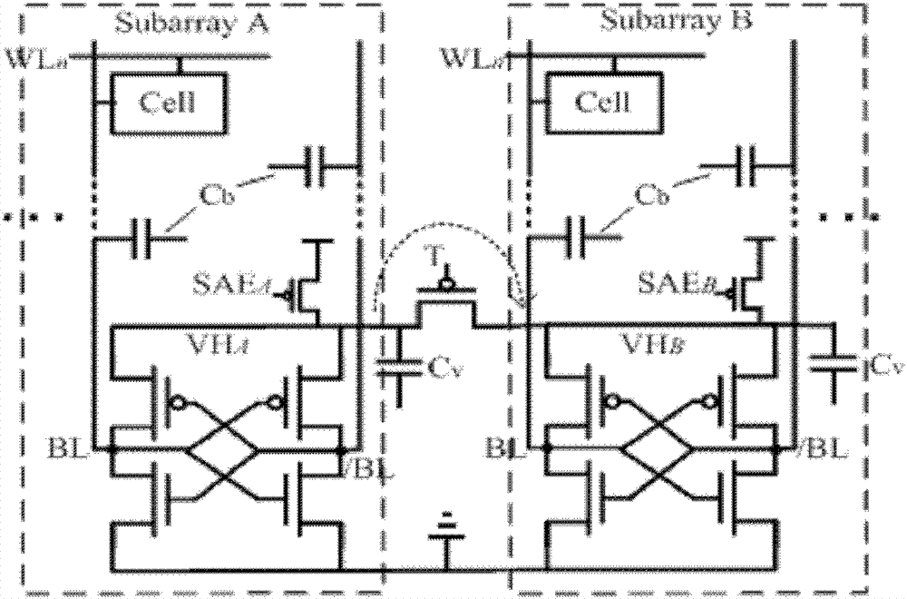
[0032] attached Figure 4 It is a schematic diagram of a compact charge transfer refresh circuit according to an embodiment of the present invention. Divide the array with a size of 128×256 into four 128×64 sub-arrays in the column direction (each sub-array is numbered 1~n), and all the sense amplifiers of each sub-array are connected to the virtual power supply terminals, which are denoted as VHn, and the sub-arrays are The virtual power terminal VHn is connected through the charge transfer switch Tn. As an example, only sub-arrays A, B, C, D are shown in the figure. It is worth noting that the embodiment here only exemplifies that the array with a size of 128×256 is divided into four 128×64 sub-arrays (each sub-array is numbered 1-n) in the column direction, and those skilled in the art can understand that it is not limited to Therefore, it can be extended to general arrays, such as dividing an array of size M*N into t M in the column direction × (N / t) sub-arrays (each su...


PUM


Abstract

The invention belongs to the technical field of memories and especially relates to a compact charge transfer refresh circuit and a refresh method thereof. The compact charge transfer refresh circuit comprises an array of M*N. The array is divided into t subarrays of M*(N / t) in a row direction. The serial numbers of the subarrays are in a range of 1 to n. Virtual power ends VHn of sense amplifiers of the subarrays are connected. Virtual power ends VHn between the subarrays are connected by charge transfer switches Tn. M, N, n and t represent natural numbers. The virtual power ends of the sense amplifiers of the subarrays are connected and VHn represents the virtual power ends. The virtual power ends VHn between the subarrays are connected by the charge transfer switches Tn. The compact charge transfer refresh circuit reduces refresh power consumption, obviously reduces refresh time, has a simple control circuit and has no additional area cost.

Description

technical field [0001] The invention belongs to the technical field of memory, and in particular relates to a compact charge transfer refresh circuit and an operation method thereof. Background technique [0002] In recent years, DRAM has been widely used in various consumer electronics products, image and video processing chips, game consoles, etc. Traditionally, the main disadvantage of DRAM in embedded device applications compared to SRAM is: the volatility of storage unit data requires refreshing, which brings additional control logic overhead and data retention power consumption overhead. Among the data retention power consumption, the dynamic power consumption caused by refresh accounts for about 30%, and this part of dynamic power consumption mainly comes from the voltage swing caused by the read and write operations of the unit on the bit line. [0003] In order to reduce the data retention power consumption of DRAM, the traditional scheme divides several groups of ...

Claims


Application Information

Patent Timeline
Patent Type & Authority Patents(China)
IPC IPC(8): G11C11/402
Inventor 解玉凤林殷茵孟超程宽
Owner FUDAN UNIV
Why Eureka
Try Eureka