Method for improving partial exposure of wafer
A local exposure and wafer technology, which is applied in the fields of electrical components, semiconductor/solid-state device manufacturing, circuits, etc., can solve the problems of insufficient coverage of wafer exposure, wafer inoperability, and affecting the success rate of machine exposure.
- Summary
- Abstract
- Description
- Claims
- Application Information
AI Technical Summary
Problems solved by technology
Method used
Image
Examples
Embodiment Construction
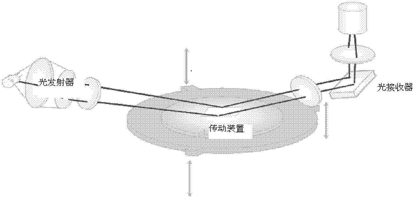
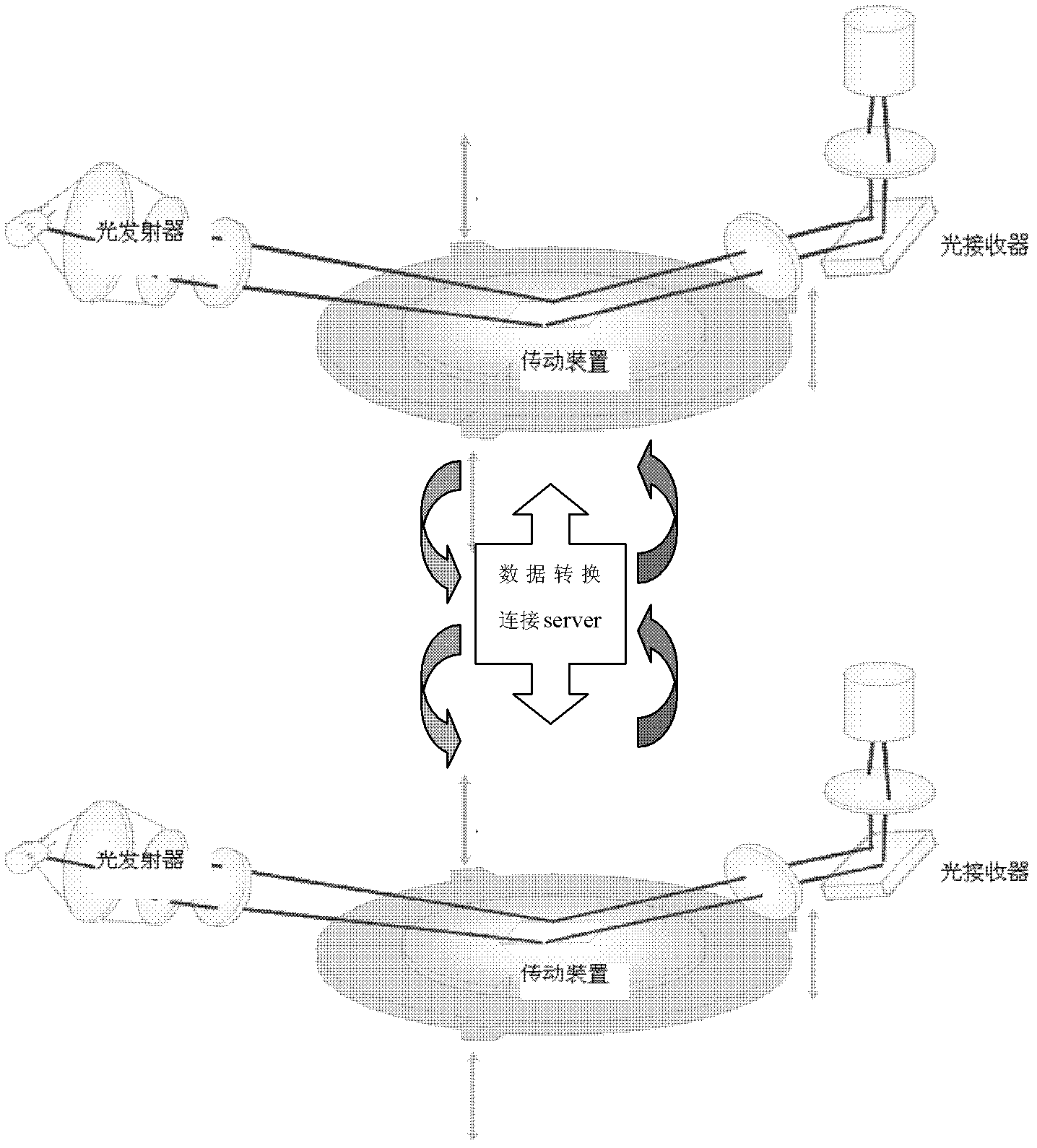
[0012] Such as figure 2 As shown, the present invention adds a stage of synchronous pre-alignment. The introduction of this stage reflects the state of the exposure stage of the machine in real time, and also uses real-time data to perform pre-focusing, leveling, and flatness corrections on the exposed wafer. This ensures that the wafer is in a relatively flat and stable state before exposure to light. The synchronous pre-alignment stage can reflect the state of the machine in real time, and at the same time, it can pre-correct the crystal surface and back conditions of the wafer.
[0013] The present invention is first established based on the exposure stage, and the parameters are basically the same. When one of the stages in the exposure stage or the pre-alignment stage moves in the X, Y, and Z directions, the server connected in the middle feeds back the previous state in real time. Monitor and correct as a benchmark to form a linkage structure. When the wafer is expose...
PUM
 Abstract
Description
Claims
Application Information

