Method for Improving Wafer Partial Exposure

A partial exposure and wafer technology, which is applied in the fields of electrical components, semiconductor/solid-state device manufacturing, circuits, etc., can solve the problem of not being able to reflect the leveling and flatness status in real time, unable to fully cover the exposure of the wafer, and affecting the success rate of machine exposure And other issues

Active Publication Date: 2016-02-10
SHANGHAI HUAHONG GRACE SEMICON MFG CORP
View PDF3 Cites 0 Cited by
  • Summary
  • Abstract
  • Description
  • Claims
  • Application Information

AI Technical Summary

Problems solved by technology

However, when the surface of the wafer is uneven due to large particles appearing on the wafer’s crystal surface or wafer back, or wafer warpage caused by processing, the machine focus cannot fully cover the exposure of the wafer caused by the difference in in-plane height.
Thus affecting the exposure success rate of the machine, if serious, it will make the wafer unable to work
[0003] The traditional method is to pre-supplement the nikon machine through regular focus, leveling and flatness detection data, but it cannot reflect the focus, leveling and flatness status of the current machine stage in real time
The state of the wafer cannot be corrected in real time during normal exposure

Method used


Image

  • Method for Improving Wafer Partial Exposure
  • Method for Improving Wafer Partial Exposure

Examples


Embodiment Construction

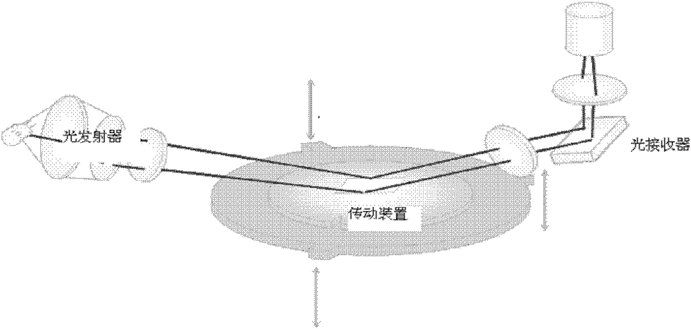
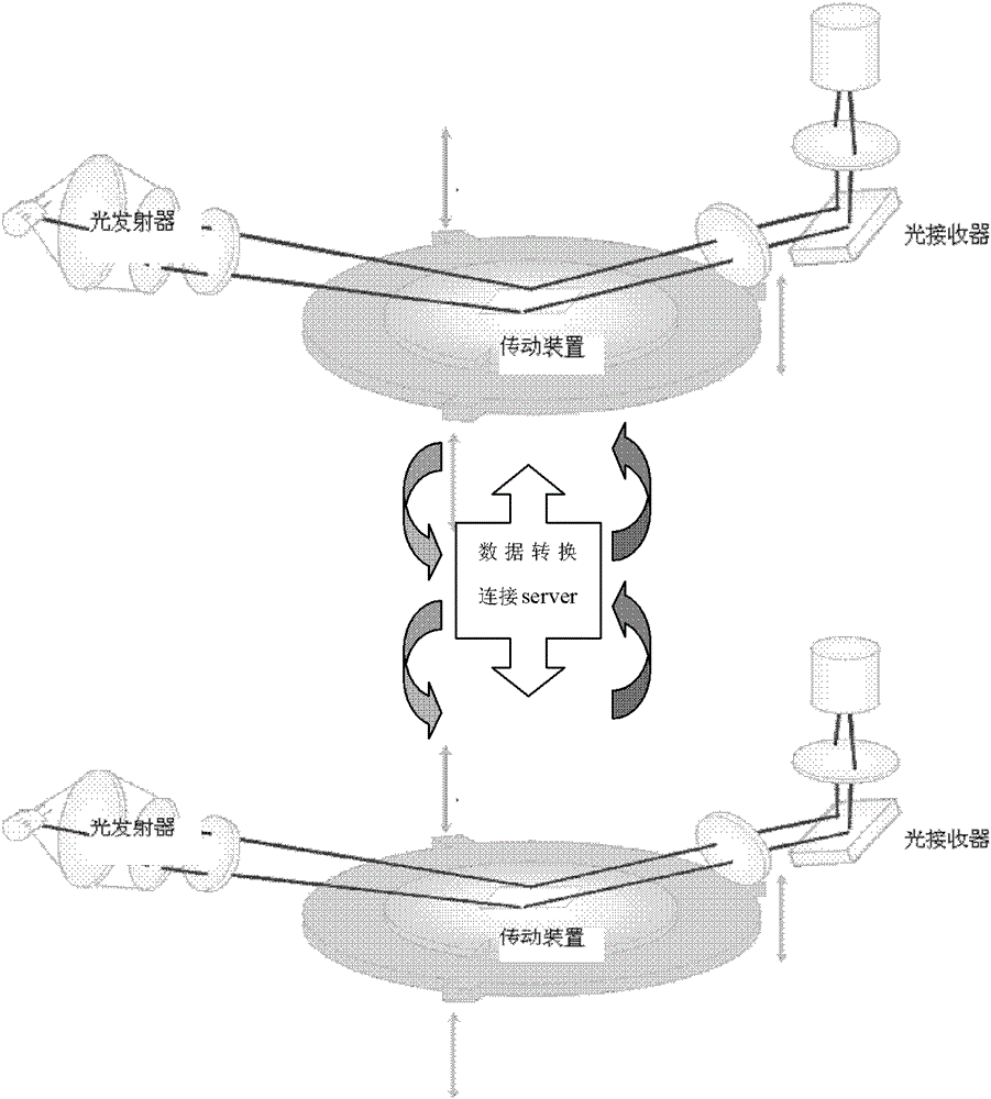
[0012] like figure 2 As shown, the present invention adds a stage of synchronous pre-alignment. The introduction of this stage reflects the state of the exposure stage of the machine in real time, and also uses real-time data to perform pre-focusing, leveling, and flatness corrections on the exposed wafer. This ensures that the wafer is in a relatively flat and stable state before exposure to light. The synchronous pre-alignment stage can reflect the state of the machine in real time, and at the same time, it can pre-correct the crystal surface and back conditions of the wafer.

[0013] The present invention is first established based on the exposure stage, and the parameters are basically the same. When one of the stages in the exposure stage or the pre-alignment stage moves in the X, Y, and Z directions, the server connected in the middle feeds back the previous state in real time. Monitor and correct as a benchmark to form a linkage structure. When the wafer is exposed, ...


PUM


Abstract

The invention discloses a method for improving partial exposure of a wafer. The method comprises conducting horizontal and flat sensing to detect conditions of a crystal face and a crystal back in advance in a synchronous pre-alignment stage; and displaying states of a machine exposure stage in real time and simultaneously conducting focusing and horizontal and flat supplementing and correcting on the exposure wafer in advance by using real-time data. The method enables the wafer to stay in a flat and stable state before exposure.

Description

technical field [0001] The present invention relates to the field of semiconductor manufacturing. Background technique [0002] like figure 1 As shown, for the machine where the wafer is currently placed, the Nikon machine is pre-supplemented through regular Focus, Leveling and Flatness detection data, and the above data is pre-supplemented to the machine. When working in the exposure stage, the pre-filled data is used to pre-align and expose the wafer. However, when the surface of the wafer is uneven due to large particles appearing on the wafer’s crystal surface or wafer back, or wafer warpage caused by processing, the machine focus cannot fully cover the exposure of the wafer caused by the difference in in-plane height. . Thereby affecting the exposure success rate of the machine, if serious, it will make the wafer unable to work. [0003] The traditional method is to pre-supplement the nikon machine through regular focus, leveling and flatness detection data, but it ...

Claims


Application Information

Patent Timeline
Patent Type & Authority Patents(China)
IPC IPC(8): H01L21/02H01L21/66
Inventor 刘金磊陈志刚陈卢佳
Owner SHANGHAI HUAHONG GRACE SEMICON MFG CORP
Why Eureka
Try Eureka