

Array substrate, display unit and control method thereof
A technology for array substrates and display devices, applied in static indicators, instruments, nonlinear optics, etc., can solve problems such as bad H-lines and affect display effects, and achieve the effect of reducing the width of the frame
- Summary
- Abstract
- Description
- Claims
- Application Information
AI Technical Summary
Problems solved by technology
Method used
Image

Examples
Embodiment 1
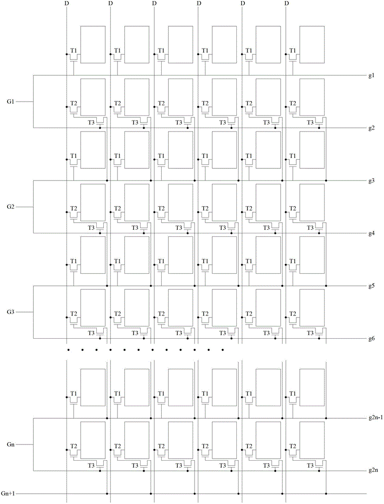
[0034] Such as figure 1 As shown, the array substrate provided by the embodiment of the present invention can be used in a liquid crystal display, and the array substrate includes n gate line groups and n+1 main gate lines G1 to Gn+1. Wherein, each main gate line is connected to the gate driver of the liquid crystal display. Each gate line group includes adjacent first gate lines and second gate lines, a first pixel group is arranged corresponding to the first gate line, and a second pixel group is arranged corresponding to the second gate line. The first pixel group includes a plurality of first pixel units arranged in rows, each first pixel unit includes a first transistor T1; the second pixel group includes a plurality of second pixel units arranged in rows, and the second pixel unit includes a second transistor T2 and switching element T3. From figure 1 It can be seen from the figure that T1, T2 and T3 are correspondingly arranged in each column of pixel units of the li...
Embodiment 2
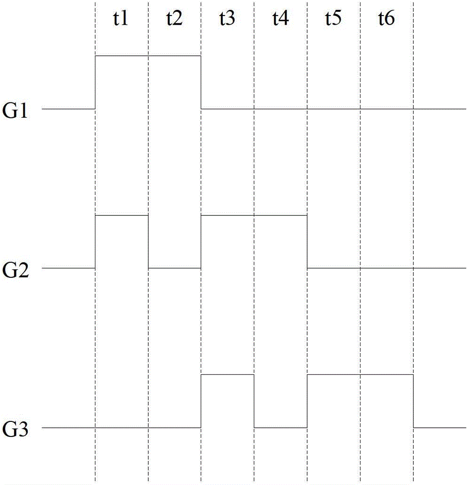
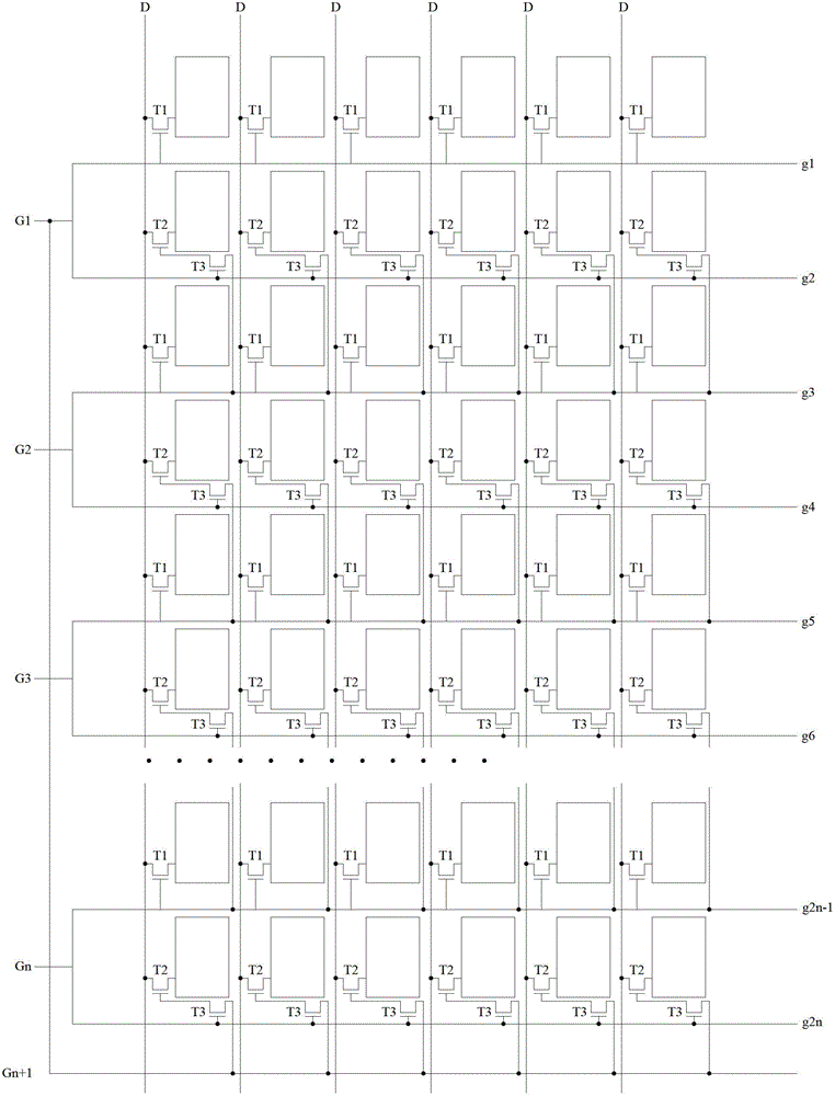
[0053] This embodiment is basically the same as Embodiment 1, the difference is: as image 3 As shown, in this embodiment, the n+1th main gate line Gn+1 is connected to the first main gate line G1. In this way, Gn+1 and G1 can be controlled together, and the timing diagram of G1 (that is, Gn+1) can be as follows Figure 4 As shown, in the two time periods before the first time period t1 in Embodiment 1, that is, within t2n-1 and t2n in the previous round of scanning, cooperate with Gn to realize the 2n-1th row and the 2nth row The pixel electrodes of the respective pixel units of the row are charged.
Embodiment 3
[0055] This embodiment is basically the same as Embodiment 1, the difference is that in this embodiment, the n+1th main gate line Gn+1 is merged into the first main gate line G1, that is, Gn+1 and G1 are combined is a main gate line as G1, then the gate (or source) of the third transistor T3 in the nth gate line group is still connected to the second gate line in the nth gate line group, but the nth gate line group The source (or gate) of T3 in the line set should be connected to G1. Specifically, it may be connected to the first gate line or the second gate line in the first gate line group.
[0056] In this way, the control method in Embodiment 2 can also be used. In addition, one busbar line can be further reduced. For example, in an HVGA liquid crystal display, only 120 busbar lines need to be arranged on both sides of the display area, which improves the symmetry of the lines on both sides of the display area.
PUM
 Abstract
Description
Claims
Application Information