Semiconductor element for thermoelectric module, and method for production thereof
A technology of thermoelectric modules and semiconductors, applied in thermoelectric device components, thermoelectric devices that only use the Peltier or Seebeck effect, etc., can solve problems such as potential difference increase
- Summary
- Abstract
- Description
- Claims
- Application Information
AI Technical Summary
Problems solved by technology
Method used
Image

Examples
Embodiment Construction
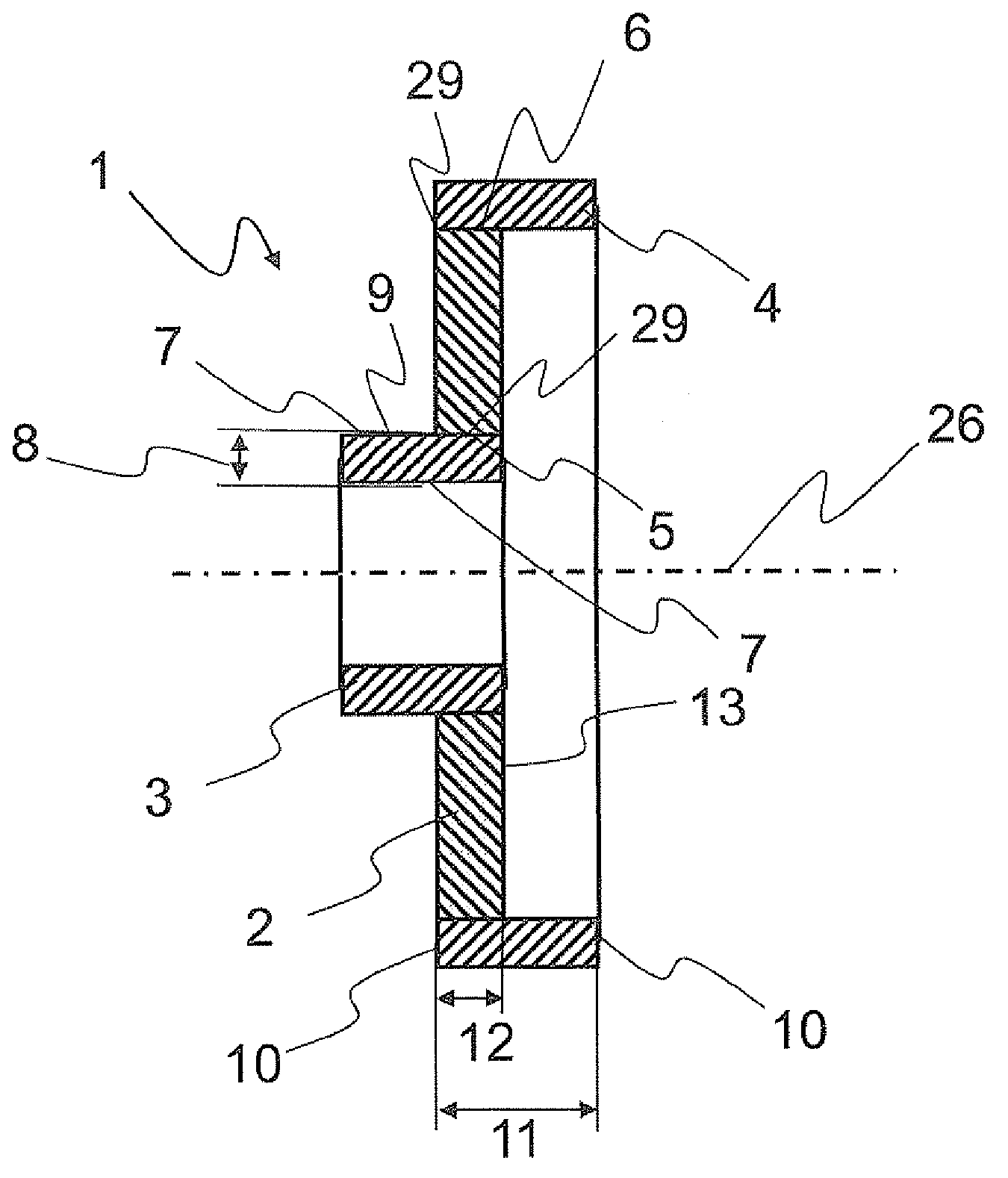
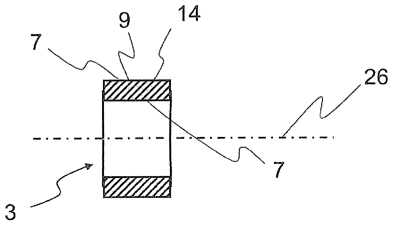
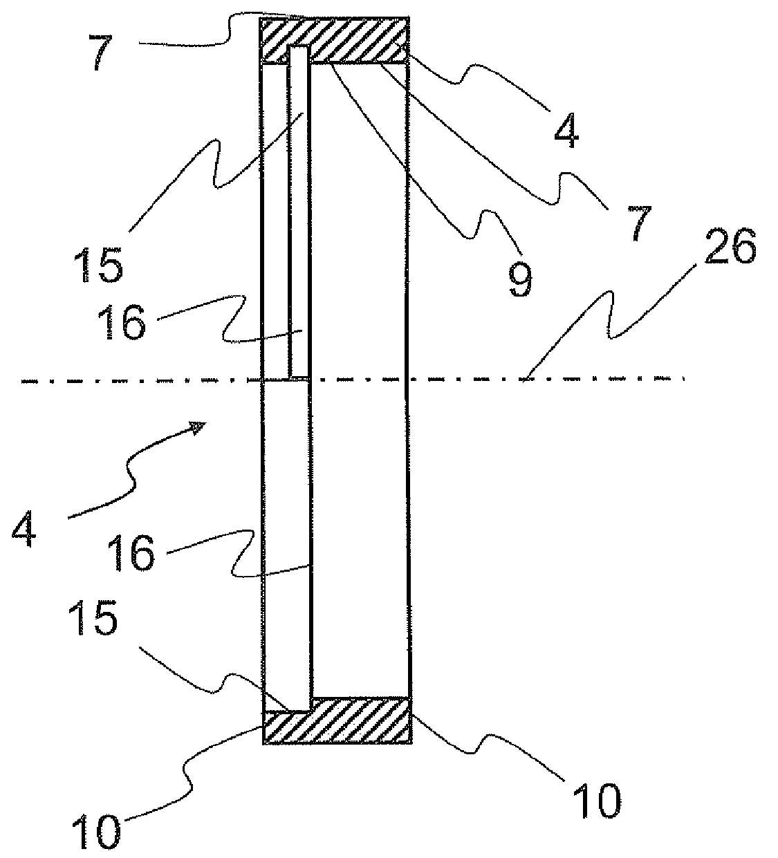
[0063] figure 1Shown is a ring-shaped semiconductor element 1 having a thermoelectric material 2 and a first frame portion 3 arranged on an inner peripheral surface 5 of the thermoelectric material 2 . The second frame portion 4 is arranged on the outer peripheral surface 6 of the thermoelectric material 2 . Even though the term "first frame portion" refers herein to the inner frame portion and the term "second frame portion" refers herein to the outer frame portion, such designations are not mandatory for various other embodiments of the present invention.
[0064] The outer peripheral surface 6 is the element surface 29 of the thermoelectric material 2 , which is opposed to the element surface 29 of the thermoelectric material 2 connected to the first frame portion 3 . The first frame part 3 has two opposite surfaces 7 , wherein an attachment surface 9 is formed on the surface 7 opposite to the thermoelectric material 2 . The thickness 8 of the first frame part 3 is formed...
PUM
| Property | Measurement | Unit |
|---|---|---|
| Roughness | aaaaa | aaaaa |
Abstract
Description
Claims
Application Information
 - Generate Ideas
- Intellectual Property
- Life Sciences
- Materials
- Tech Scout
- Unparalleled Data Quality
- Higher Quality Content
- 60% Fewer Hallucinations
Browse by: Latest US Patents, China's latest patents, Technical Efficacy Thesaurus, Application Domain, Technology Topic, Popular Technical Reports.
© 2025 PatSnap. All rights reserved.Legal|Privacy policy|Modern Slavery Act Transparency Statement|Sitemap|About US| Contact US: help@patsnap.com