Check patentability & draft patents in minutes with Patsnap Eureka AI!

Substrate processing device and method

A processing device and processing method technology, applied in the direction of electrical components, semiconductor/solid-state device manufacturing, circuits, etc., can solve the problems of reduced productivity, inability to process faster than a certain speed, cracks in semiconductor wafers, etc.

Active Publication Date: 2013-07-03
SHIBAURA MECHATRONICS CORP
View PDF4 Cites 9 Cited by
  • Summary
  • Abstract
  • Description
  • Claims
  • Application Information

AI Technical Summary

Problems solved by technology

In addition, since the above-mentioned stress relief step or cleaning step is required as an additional step, the process is complicated, so there is a problem such as a decrease in productivity.
In addition, although the processing efficiency of the grinding process is high, it may cause cracks in the semiconductor wafer, so there is also a problem that the processing speed cannot be made more than a certain value.

Method used


Image

  • Substrate processing device and method
  • Substrate processing device and method
  • Substrate processing device and method

Examples


no. 1 approach

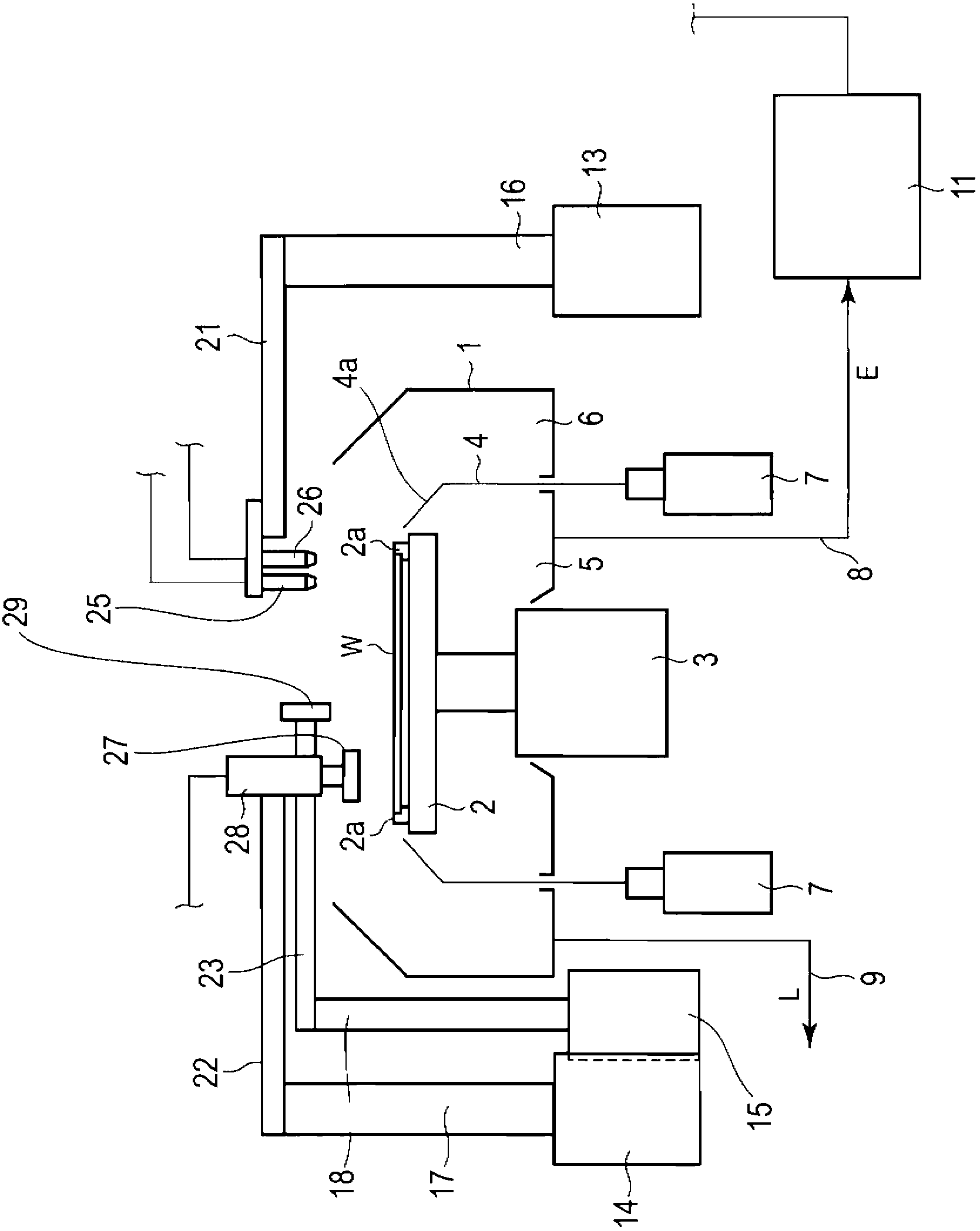
[0031] figure 1 with figure 2 A spin processing device is shown as a processing device, and the spin processing device includes a cup body 1 . A rotary table 2 is provided inside the cup body 1 . The rotary table 2 is rotationally driven by a table drive source 3 , and on the upper surface of the rotary table 2 , a semiconductor wafer W serving as a substrate is held horizontally and detachably by a plurality of holding pins 2 a. That is, the semiconductor wafer W is held on the rotary table 2 so as to rotate integrally with the rotary table 2 .

[0032] Such as figure 1 As shown, in the inside of the above-mentioned cup body 1, there is provided a cylindrical partition body 4 that partitions the interior into an inner space portion 5 and an outer space portion 6, and the partition body 4 is driven in the vertical direction by a plurality of vertical driving sources 7. .

[0033] When the spacer 4 is at the raised position, the etchant E, which is supplied to the upper s...


PUM


Abstract

The invention provides a substrate processing device and method capable of etching faces of semi-conductor chips based on etching liquid. The substrate processing device is provided with a first nozzle (25) supplying etching liquid to the plate face of the semi-conductor chip (W); a thickness detection sensor (29) detecting thickness of the semi-conductor chip etched by the etching liquid; a control device interrupting etching based on the etching liquid when thickness of the semiconductor chip detected by the thickness detection sensor is abnormal; and a grinding body (27) processing the plate face of the semiconductor chip to a rough face when the etching based on the etching liquid is interrupted.

Description

technical field [0001] The present invention relates to a substrate processing device and processing method for etching the surface of a substrate such as a semiconductor wafer using an etchant. Background technique [0002] For example, in the manufacturing process of a semiconductor device, an etching process of removing an oxide film, a nitride film, an aluminum film, etc. formed on the surface of a semiconductor wafer using an etchant is known. [0003] In the case of removing the film formed on the surface of the semiconductor wafer with an etchant, in order to make the film thickness a set thickness, conventionally, the etching process is performed for a preset time, or the thickness is detected by a film thickness sensor. The thickness of the semiconductor wafer is etched, and the semiconductor wafer is etched to a desired thickness. [0004] Furthermore, depending on the processing in the post-process, it may be necessary to form a rib shape or the like on the outer...

Claims


Application Information

Patent Timeline
IPC IPC(8): H01L21/67H01L21/3105H01L21/321
CPCH01L21/31111H01L21/32134H01L21/6708
Inventor 林航之介松井绘美大田垣崇桧森洋辅
Owner SHIBAURA MECHATRONICS CORP
Features
  • R&D
  • Intellectual Property
  • Life Sciences
  • Materials
  • Tech Scout
  • Unparalleled Data Quality
  • Higher Quality Content
  • 60% Fewer Hallucinations
Learn More