
Eureka
For R&D, Eureka makes reading and utilizing patents & technical documents easy.
Eureka AIR
Designed for self-driven R&D workflows. Generate viable solutions, solve complex R&D challenges, empower your innovation with AI.

Eureka Materials
Designed for material experts only. Revolutionize your material R&D, from search, analyze, to developing new materials.

TechResearch
Generate reliable direction feasibility study reports for your R&D in just a few steps.

TechSeek
Discover and master advanced knowledge NOW. Basics, ideas, possibilities, all at once.

TechMind
As an expert in R&D Theories, TechMind can generates customized viable solutions instantly.

TechRisk
Analyze your overall solution with one click, know your potential R&D risks in advance.

TechMonitor
Get weekly tech updates, stay abreast of the latest tech innovations and key insights.
Driving method and pixel units of active matrix organic light emitting diode panel
A technology of light-emitting diodes and active matrix, applied in instruments, static indicators, etc., can solve the problems of poor brightness uniformity of active matrix organic light-emitting diode panels, variation of transistor M200 drive current, etc., to solve uneven brightness and improve display The effect of uniform quality and brightness
- Summary
- Abstract
- Description
- Claims
- Application Information
AI Technical Summary
Problems solved by technology
Method used
Image

Examples
Embodiment Construction
[0033] In order to further illustrate the technical means adopted by the present invention and its effects, the following describes in detail in conjunction with preferred embodiments of the present invention and accompanying drawings.
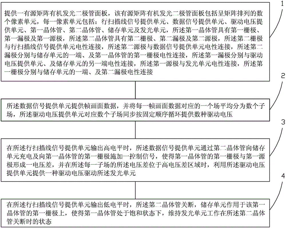
[0034] see Figures 3 to 6 , the present invention provides a driving method for an active matrix organic light emitting diode panel, comprising the following steps:
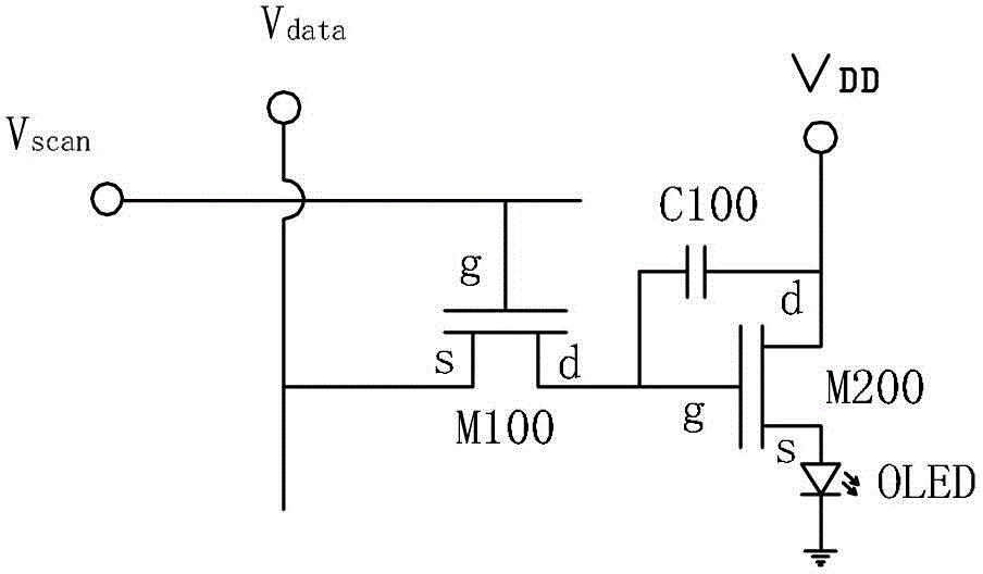
[0035] Step 1, provide an active matrix organic light emitting diode panel, the active matrix organic light emitting diode panel includes several pixel units 20 arranged in a matrix, each pixel unit 20 includes: a row scan line signal supply unit 22, a data signal The supply unit 24 , the driving voltage supply unit 26 , the first transistor M1 , the second transistor M2 , the storage unit 27 and the light emitting unit 28 .
[0036] The first transistor M1 has a first gate g, a first source s, and a first drain d, and the second transistor M2 has a second gate g, a second drai...
PUM
 Abstract
Description
Claims
Application Information
 - R&D Engineer
- R&D Manager
- IP Professional
- Industry Leading Data Capabilities
- Powerful AI technology
- Patent DNA Extraction
Browse by: Latest US Patents, China's latest patents, Technical Efficacy Thesaurus, Application Domain, Technology Topic, Popular Technical Reports.
© 2024 PatSnap. All rights reserved.Legal|Privacy policy|Modern Slavery Act Transparency Statement|Sitemap|About US| Contact US: help@patsnap.com