
Organic light emitting display

a light-emitting display and organic technology, applied in the field of organic light-emitting display, can solve the problems of inability to display an image of a desired (or uniform) luminance, a long time to charge a data line, and a relatively heavy and bulky display. achieve the effect of fast response tim

Active Publication Date: 2007-02-01
SAMSUNG DISPLAY CO LTD +1
View PDF10 Cites 74 Cited by
  • Summary
  • Abstract
  • Description
  • Claims
  • Application Information

AI Technical Summary

Benefits of technology

[0014] Accordingly, it is an aspect of the present invention to provide an organic light emitting display device capable of displaying an image of uniform brightness with a fast response time.

Problems solved by technology

Recently, various flat panel display devices have been developed to substitute for a cathode ray tube (CRT) display because the CRT display is relatively heavy and bulky.
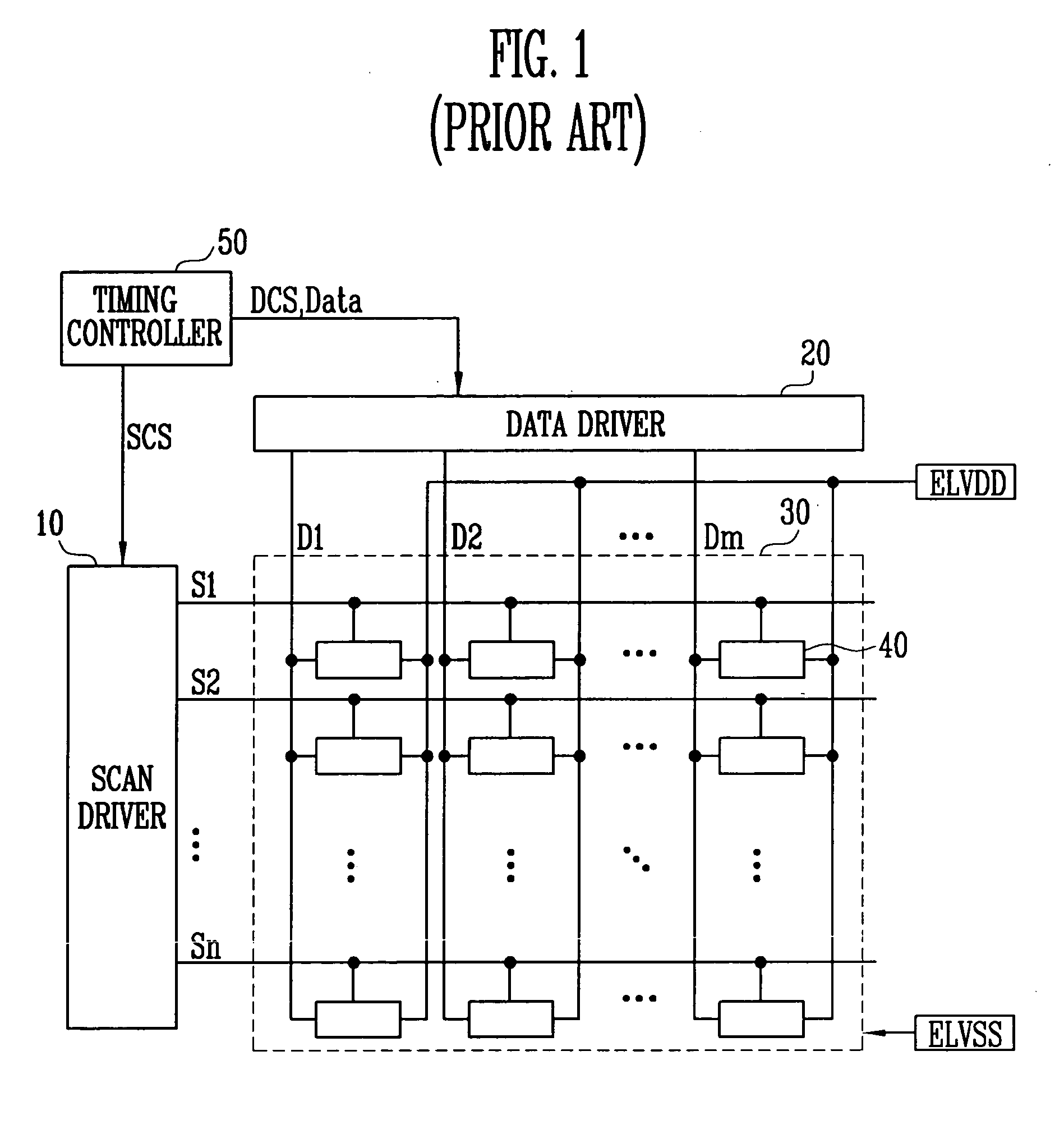
However, due to non-uniformity of threshold voltages and a deviation of electron mobility of transistors included in each pixel 40, the conventional organic light emitting display device has a problem in that it cannot display an image of a desired (or uniform) luminance.
However, because the current supplied as the data signal is a minute current, it takes a long time to charge a data line.
Upon considering one (1) horizontal period of several tens μs, a charge time of several ms may be too long.

Method used


Image

  • Organic light emitting display
  • Organic light emitting display
  • Organic light emitting display

Examples


first embodiment

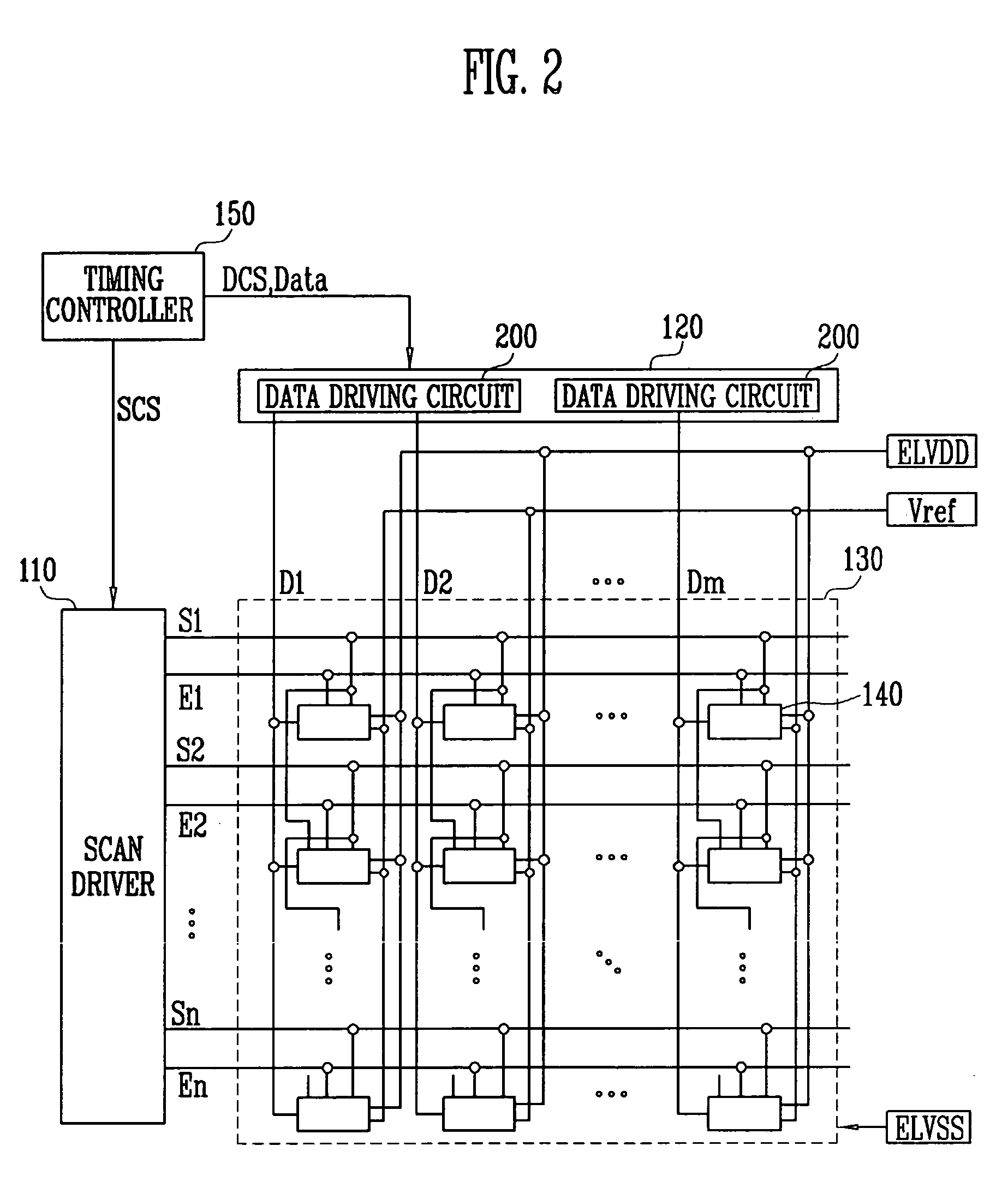
[0037] With reference to FIG. 2, the organic light emitting display device according to the present invention includes a display region 130, a scan driver 110, a data driver 120, and a timing controller 150. The display region 130 includes a plurality of pixels 140 that are coupled with scan lines S1 to Sn, light emitting control lines E1 to En, and data lines D1 to Dm. The scan driver 110 drives the scan lines S1 to Sn, and the light emitting control lines E1 to En. The data driver 120 drives the data lines D1 to Dm. The timing controller 150 controls the scan driver 110 and the data driver 120.

[0038] The display region 130 has pixels 140 that are formed at an area divided by the scan lines S1 to Sn, the light emitting control lines E1 to En, and the data lines D1 to Dm. Each of the pixels 140 receives a first power of a first power supply EVVDD, a second power of a second supply ELVSS, and a reference power of a reference power supply Vref from an exterior. Upon receiving the refe...

second embodiment

[0078] On the other hand, as shown in FIG. 7, the data driving circuit 200 of the present invention further includes a level shifter 300 connected to (or installed at a next stage of) the holding latch 230. The level shifter 300 increases a voltage level of data supplied from the holding latch 230, and provides the data having the increased voltage level to the DAC 250. When data having a higher voltage level from an external system is supplied to the data driving circuit 200, a circuit component having high resisting potential according to the voltage level should be installed, thereby causing an increase in a manufacturing cost. Accordingly, in FIG. 7, data having a lower voltage level is supplied to the data driving circuit 200 from an, external system. The level shifter 300 boosts the data having a lower voltage level to a higher voltage level such that the circuit component having high resisting potential is not needed.

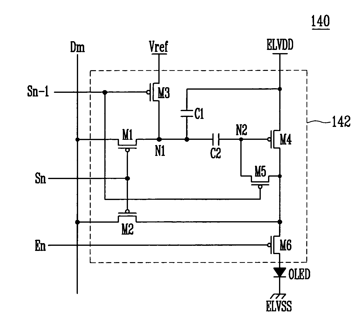
[0079]FIG. 8 is a view showing an example of a connected re...

fourth embodiment

[0125]FIG. 14 is a view showing an organic light emitting display device according to the present invention. In FIG. 14, elements that are substantially the same as those shown in FIG. 2 are allotted the same reference numerals, and the description of the same elements will be omitted.

[0126] With reference to FIG. 14, the organic light emitting display device according to the fourth embodiment of the present invention includes a voltage generator 330 and a subtracter 332.

[0127] The voltage generator 330 receives a vertical sync signal Vsync and a horizontal sync signal Hsync. Every time the horizontal sync signal is inputted to the voltage generator 332, the voltage generator 330 generates and provides a voltage increasing in a stepped form to the subtracter 332. Upon receiving the vertical sync signal Vsync, the voltage generator 330 is initialized.

[0128] An operation of the voltage generator 330 having the construction mentioned above will be illustrated by reference to FIG. 15 ...


PUM


Abstract

An organic light emitting display device capable of displaying an image of uniform brightness. A scan driver drives scan lines and light emitting control lines that are formed parallel to each other. A data driver drives data lines formed at a direction intersecting the scan lines and the light emitting control lines, and pixels are disposed to be coupled with the scan lines, the light emitting control lines, and the data lines. An auxiliary line is formed parallel to the data lines. One side of the auxiliary line is coupled with a reference power supply and another side of the auxiliary line is coupled with a current source. Connectors are disposed at crossing areas of the auxiliary line and the scan lines. A voltage transfer unit is coupled with the connectors and transfers a voltage supplied to the connectors to the data driver.

Description

CROSS-REFERENCE TO RELATED APPLICATION [0001] This application claims priority to and the benefit of Korean Patent Application No. 10-2005-0070434, filed on Aug. 1, 2005, in the Korean Intellectual Property Office, the entire content of which is incorporated herein by reference. BACKGROUND [0002] 1. Field of the Invention [0003] The present invention relates to an organic light emitting display, and more particularly to an organic light emitting display that can display an image of uniform brightness. [0004] 2. Discussion of Related Art [0005] Recently, various flat panel display devices have been developed to substitute for a cathode ray tube (CRT) display because the CRT display is relatively heavy and bulky. Flat panel display devices include liquid crystal displays (LCDs), field emission displays (FEDs), plasma display panels (PDPs), organic light emitting display devices, etc. [0006] An organic light emitting display device is a flat display device that displays an image using ...

Claims


Application Information

Patent Timeline
Patent Type & Authority Applications(United States)
IPC IPC(8): G09G3/30H05B44/00
CPCG09G3/3233G09G3/3283G09G3/3291G09G2300/0819G09G2300/0852G09G2330/02G09G2310/0251G09G2310/027G09G2310/0289G09G2320/0223G09G2320/043G09G2300/0861G09G3/30G09G3/20G09G3/32
Inventor RYU, DO HYUNGCHUNG, BO YONGKWON, OH KYONG
Owner SAMSUNG DISPLAY CO LTD
Learn More