Wafer prealignment device
A pre-alignment and wafer technology, applied in electrical components, semiconductor/solid-state device manufacturing, circuits, etc., can solve problems such as inability to clamp wafers, unbalanced wafers, and uneven force
- Summary
- Abstract
- Description
- Claims
- Application Information
AI Technical Summary
Problems solved by technology
Method used
Image
Examples
Embodiment Construction
[0028] The above-mentioned wafer pre-alignment device is further described below through specific embodiments and drawings.
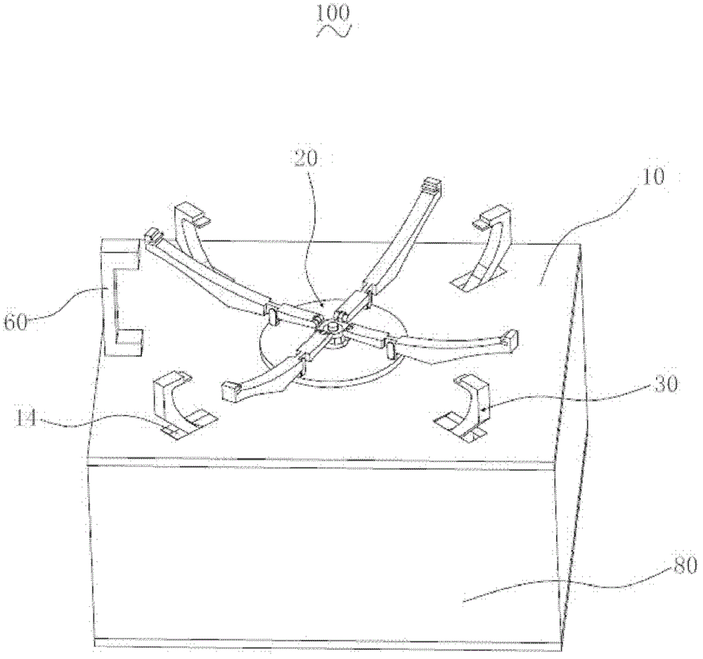
[0029] See also figure 1 , figure 2 with Figure 5 , The wafer pre-alignment device 100 of an embodiment includes a substrate 10, a first supporting device 20, a second supporting device 30, a first driving device 40, a second driving device 50, a sensor 60, and a control unit (not shown) ), bearing 70 and protective box 80.
[0030] The substrate 10 is approximately a rectangular plate, and a first through hole 12 and a plurality of second through holes 14 are opened on the substrate 10. The first through hole 12 is opened in the middle of the substrate 10, and the second through hole 14 is located around the first through hole 12. In this embodiment, the number of the second through holes 14 is four.
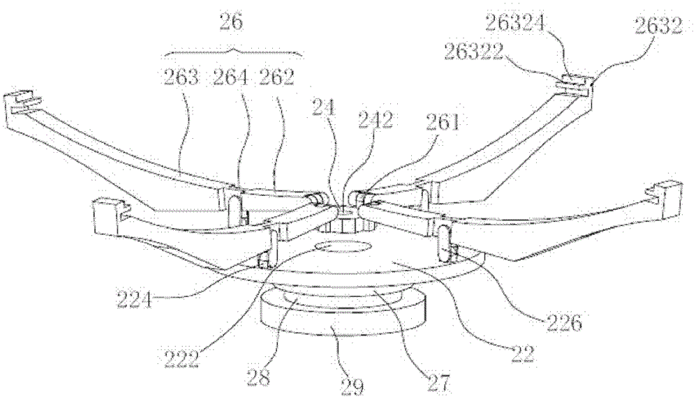
[0031] See image 3 , The first supporting device 20 includes a supporting base 22, a connector 24 and four first supporting arms 26.
[0032] The support b...
PUM
 Abstract
Description
Claims
Application Information


