Through silicon via (TSV) exposure process

A process and semiconductor technology, applied in the field of microelectronics, can solve problems such as unmet requirements and problems with TSV electrical connection

Active Publication Date: 2013-07-24
NAT CENT FOR ADVANCED PACKAGING
View PDF3 Cites 8 Cited by
  • Summary
  • Abstract
  • Description
  • Claims
  • Application Information

AI Technical Summary

Problems solved by technology

The result of this is that after the etching is completed, the heights of TSV outcrops in different regions are different. The height of TSV outcrops in some places may meet the requirements, while the height of TSV outcrops in some places may not meet th

Method used


Image

  • Through silicon via (TSV) exposure process
  • Through silicon via (TSV) exposure process
  • Through silicon via (TSV) exposure process

Examples


Embodiment Construction

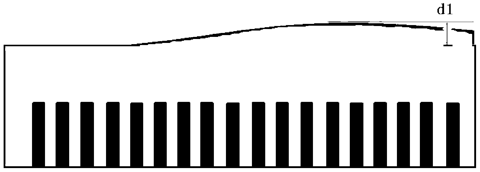
[0023] As mentioned in the background technology, in the existing TSV outcropping process, when the mechanical grinding machine is grinding, the thickness variation (TTV) d1 of the wafer surface is controlled at 2.5 microns, and this variation will be wet ( / dry) in the next step In the method etching outcrop, it is maintained due to the isotropy of the etching. As a result, after the etching is completed, the heights of the TSV outcrops in different regions are different, and the height of the TSV outcrop in some places may meet the requirements, while the height of the TSV outcrop in some places may not meet the requirements. Taking the outcrop height of 10 μm as an example, in the thicker areas of the wafer, the exposed copper may only be 7-8 μm, which will cause problems in the subsequent electrical connection of TSVs in these areas.

[0024] Therefore, in response to these problems, the present invention proposes a new TSV outcropping process, which can not only avoid the ...


PUM


Abstract

The invention discloses a through silicon via (TSV) exposure process. After the back surface of a wafer substrate is ground and thinned mechanically, a chemical mechanical polishing (CMP) process is performed twice. In the first CMP process, a polishing solution without selection ratio is adopted, so that the total thickness variation (TTV) of the surface of the substrate is controlled to be less than 1 mu m, and the problem of low exposure uniformity caused by over-large TTV is solved. In the second CMP process, a polishing solution with high selection ratio among the substrate, a TSV medium layer and a TSV barrier layer is adopted, so that the etching is stopped at the TSV barrier layer, an internal conductive copper column is protected from being corroded, the etched substrate appearance is of a transition structure for the deposition of a seed layer, and the stability of a TSV during subsequent electric connection is improved.

Description

technical field [0001] The invention relates to a method for manufacturing or processing semiconductor or solid devices or parts thereof in the technical field of microelectronics, in particular to a TSV outcropping process for transmitting current between separate components in a microelectronic device by using metal 3D interconnection. Background technique [0002] With the continuous advancement of microelectronics technology, the feature size of integrated circuits has been continuously reduced and the interconnection density has been continuously increased. At the same time, users' requirements for high performance and low power consumption continue to increase. In this case, the way to improve the performance by further reducing the line width of the interconnection is limited by the physical characteristics of the material and the equipment process, and the resistance-capacitance (RC) delay of the two-dimensional interconnection gradually becomes the limit to improve ...

Claims


Application Information

Patent Timeline
IPC IPC(8): H01L21/768
Inventor 顾海洋张文奇宋崇申
Owner NAT CENT FOR ADVANCED PACKAGING
Why Eureka
Try Eureka