Silicon wafer linear exchange device and method

An exchange device, straight line technology, applied in the direction of exposure device, transportation and packaging, conveyor objects, etc. in the photoengraving process, which can solve the problems of low precision and low work efficiency

Active Publication Date: 2013-12-04
SHANGHAI MICRO ELECTRONICS EQUIP (GRP) CO LTD +1
View PDF2 Cites 15 Cited by
  • Summary
  • Abstract
  • Description
  • Claims
  • Application Information

AI Technical Summary

Problems solved by technology

[0007] The object of the present invention is to provide a silicon chip linear exchange device and method to solve the problems of low working efficiency and low precision of the existing silicon chip linear exchange device

Method used


Image

  • Silicon wafer linear exchange device and method
  • Silicon wafer linear exchange device and method
  • Silicon wafer linear exchange device and method

Examples


Embodiment Construction

[0035] In order to make the above objects, features and advantages of the present invention more comprehensible, specific implementations of the present invention will be described in detail below in conjunction with the accompanying drawings.

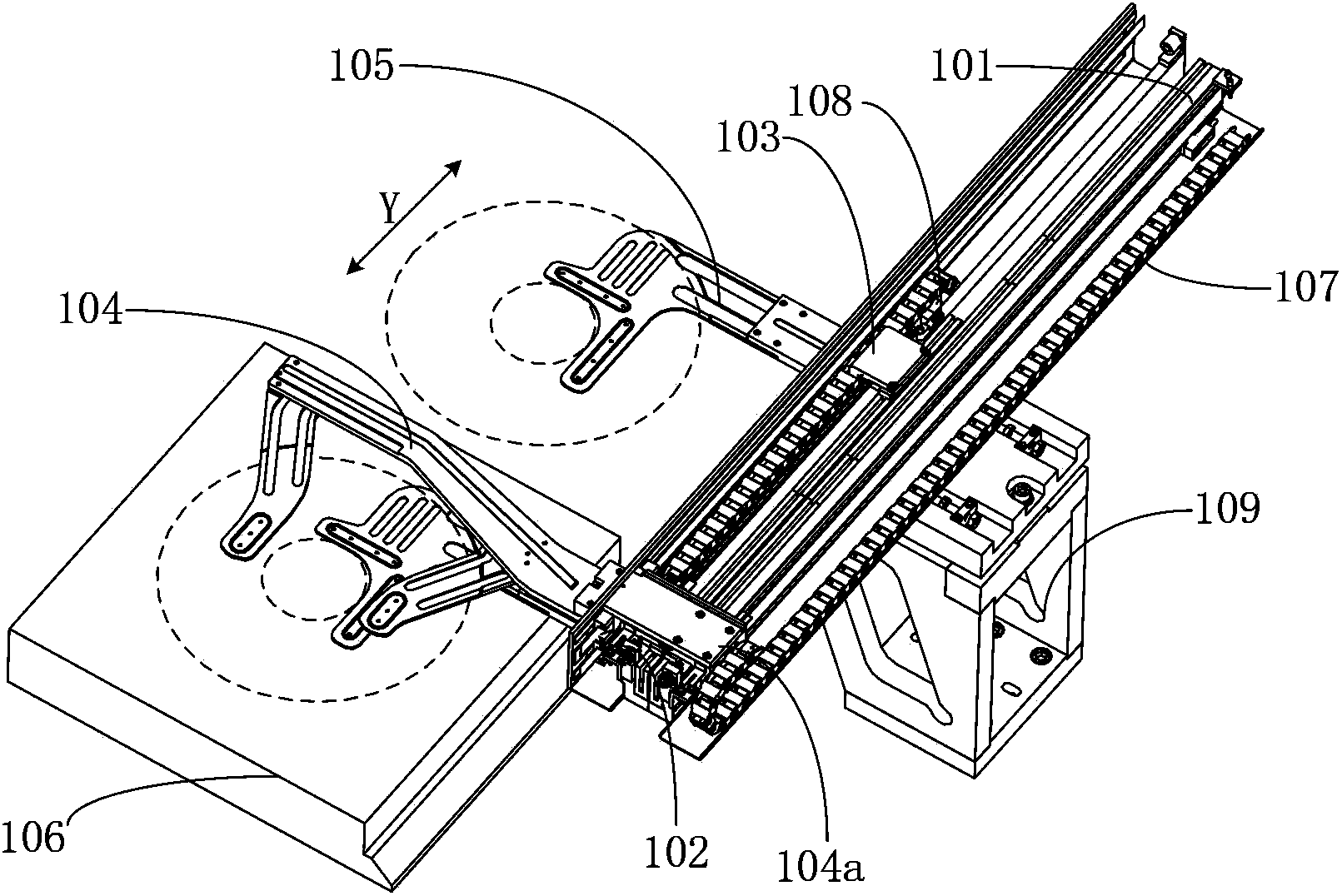
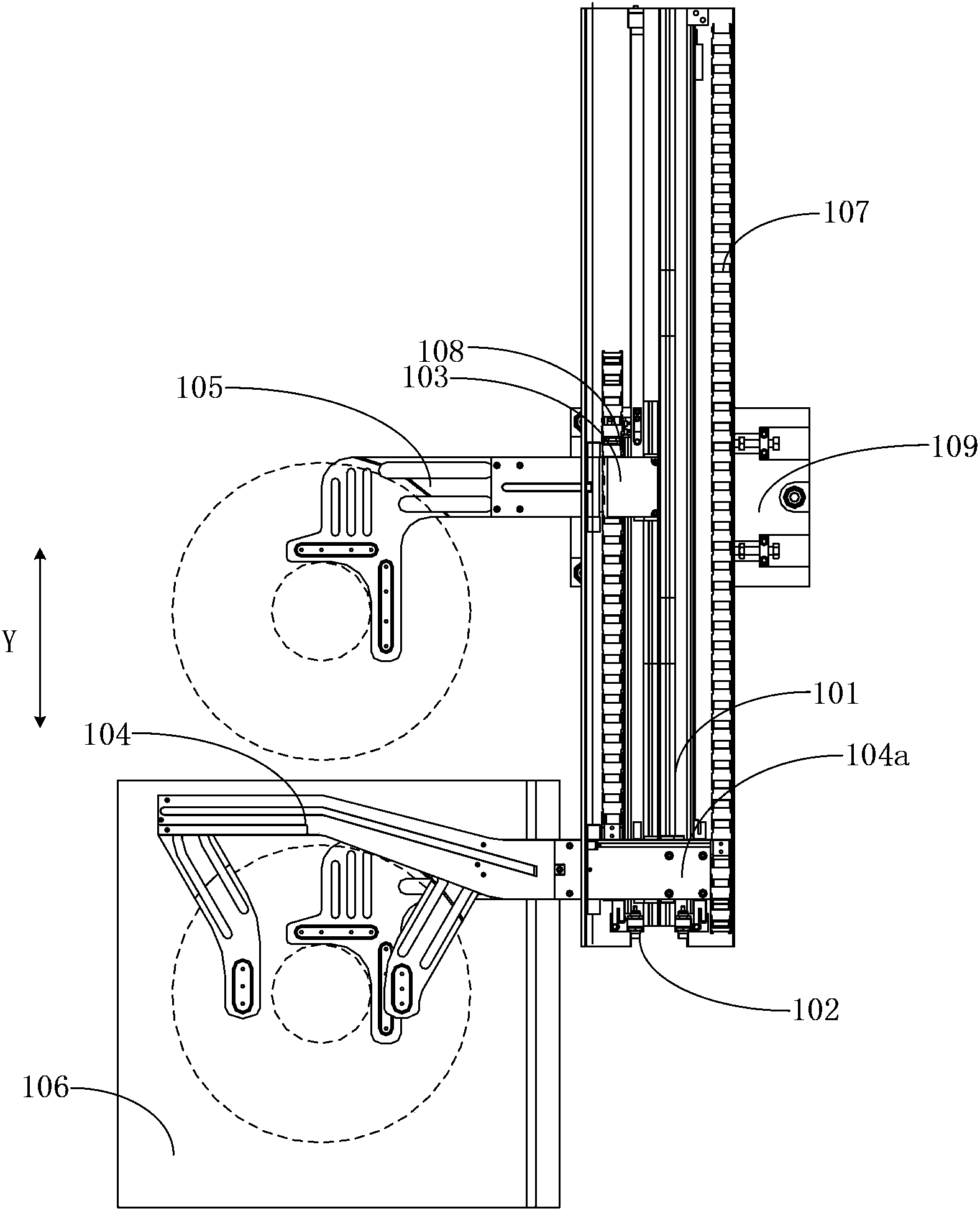
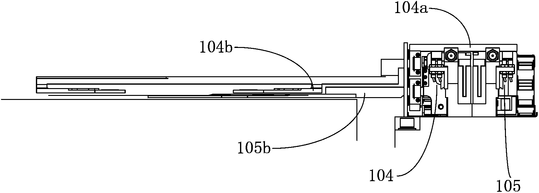
[0036] The silicon chip linear exchange device provided by the present invention is used to transfer materials between the workbench and the external device, and its structure is as follows: figure 1 and figure 2 As shown, the guide rail 101 is included, specifically, the guide rail 101 is a single wide linear guide rail; the first slider 102 and the second slider 103 arranged on the guide rail 101, the first and second The sliders 102, 103 are capable of staggered reciprocating motion along the guide rail 101; the first mechanical arm 104, the first mechanical arm 104 is connected to the first slider 102 through the mechanical arm adapter 104a; and the second mechanical arm 105, the second mechanical arm 105 is connected to the seco...


PUM

PropertyMeasurementUnit
thicknessaaaaaaaaaa
thicknessaaaaaaaaaa

Abstract

The invention relates to the field of lithography device, and especially relates to a silicon wafer linear exchange device and a method adopting the device. The method and device are used for delivering materials between a workbench and an external device. The device comprises a guide rail, a first slide block and a second slide block arranged on the guide rail, a first mechanical arm connected with the first slide block through a mechanical arm connection connector; and a second mechanical arm connected with the second slide block. The first and second slide blocks can perform staggered reciprocating movements along the guide rail. The first and second mechanical arms are positioned in two different movement planes which are parallel. The invention adopts an avoidance design, such that the first and second mechanical arms move in two parallel planes, such that the two sets of mechanical arms run from opposite directions. When the first mechanical arm exchange silicon wafer with the work bench, the second mechanical arm simultaneously carries out silicon wafer exchange with a manipulator. When the exchange is finished, the two sets of mechanical arms perform reverse movements simultaneously, and next exchange is carried out. Therefore, half of movement exchange time is reduced.

Description

technical field [0001] The invention relates to the field of photolithography equipment, in particular to a device and method for linearly exchanging silicon wafers. Background technique [0002] The silicon wafer transmission system is used in many semiconductor equipment such as lithography equipment. As the external material interface of these equipments, it must be reliable and efficient, and can provide a certain material transmission accuracy, which refers to the silicon wafer. The transfer system can transfer the material to the workbench with a specified attitude and maintain a certain accuracy, which can greatly reduce the time for the workbench to find the reference mark of the silicon wafer under the alignment system, and what is more, after the transfer is completed, the alignment The system can directly capture the mark without scanning the mark through the movement of the workbench, which greatly improves the working efficiency of this type of equipment, improv...

Claims


Application Information

Patent Timeline
Patent Type & Authority Applications(China)
IPC IPC(8): G03F7/20H01L21/677
Inventor 王邵玉田耀杰姜杰黄春霞
Owner SHANGHAI MICRO ELECTRONICS EQUIP (GRP) CO LTD
Why Eureka
Try Eureka