
Liquid crystal display device as well as pixel structure and driving method thereof

一种像素结构、像素电极的技术,应用在静态指示器、非线性光学、仪器等方向,能够解决Crosstalk成效不佳、受限扫描方式、面板充电不足等问题,达到保证充电时间、解析度高、降低3D串扰的效果

Active Publication Date: 2013-12-25
TCL CHINA STAR OPTOELECTRONICS TECH CO LTD
View PDF5 Cites 9 Cited by
  • Summary
  • Abstract
  • Description
  • Claims
  • Application Information

AI Technical Summary

Problems solved by technology

However, the above two methods currently have certain limitations
[0004] Among them, the first method is limited by its scanning method, which requires the BLU to be designed only for single short or double short, and the effect of improving Cross talk is not good.
The second method requires a higher refresh rate, usually 240Hz, because it needs to insert a black frame when the left and right eye signals are switched, which will reduce the charging time to half of 120Hz, causing the panel to be insufficiently charged risk, which in turn leads to the appearance of spots (Mura), which greatly affects the quality of liquid crystal display devices

Method used


Image

  • Liquid crystal display device as well as pixel structure and driving method thereof
  • Liquid crystal display device as well as pixel structure and driving method thereof
  • Liquid crystal display device as well as pixel structure and driving method thereof

Examples


Embodiment Construction

[0025] The present invention will be described in detail below in conjunction with the accompanying drawings and embodiments.

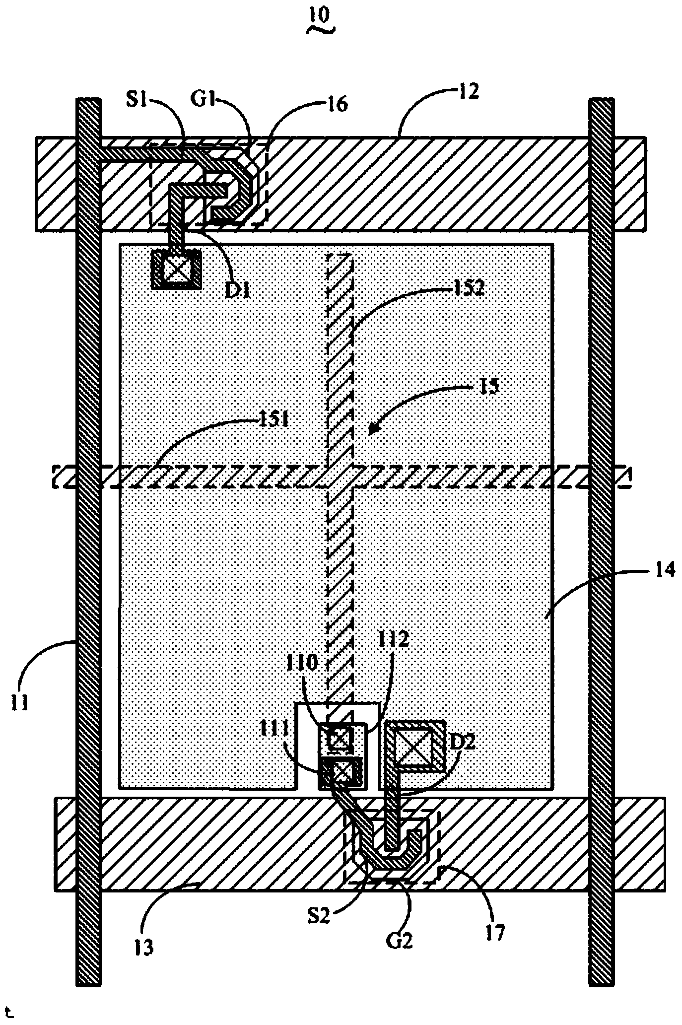
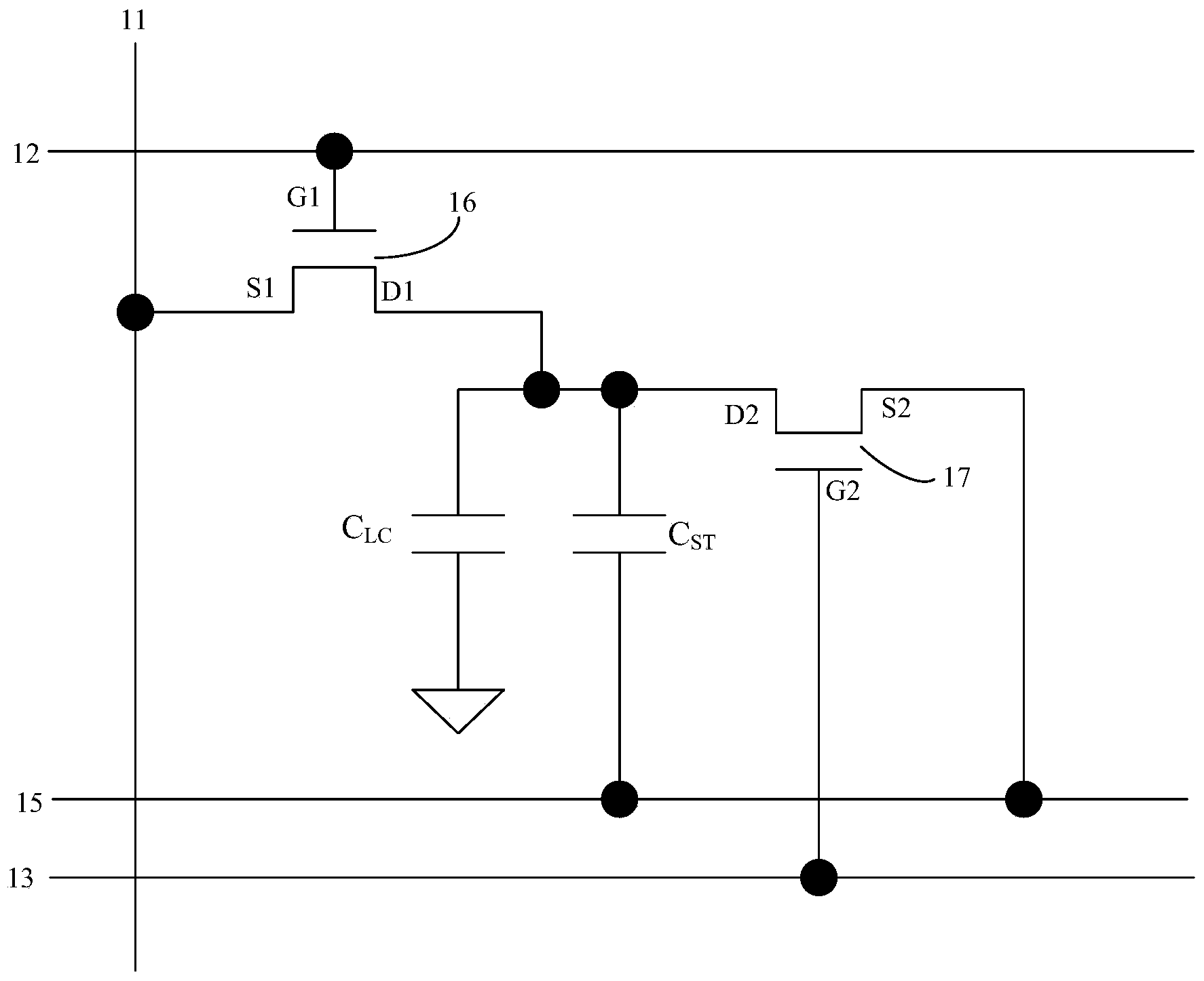
[0026] see figure 1 and figure 2 , figure 1 is a structural schematic diagram of an embodiment of the pixel structure of the present invention, figure 2 yes figure 1 Equivalent circuit diagram of the pixel structure shown. Such as figure 1 and figure 2 As shown, the pixel structure 10 of the present invention includes a data line 11, a first scan line 12 vertically intersecting with the data line 11, a second scan line 13 arranged parallel to the first scan line 12, a second scan line 13 arranged between the first scan line 12 and The pixel electrode 14 between the second scanning line 13 and the common electrode line 15 for providing a common voltage. The second switch unit 17 is electrically connected.

[0027] In this embodiment, the gate G1 of the first switch unit 16 is electrically connected to the first scanning line 12, the source S...


PUM


Abstract

The invention discloses a liquid crystal display device as well as a pixel structure and a driving method thereof. According to the pixel structure, a first scanning line of the pixel structure transmits a first scanning signal for starting a first switching unit to charge a pixel electrode; when the charging is finished and the pixel electrode is at an electric quantity keeping state, a second scanning line transmits a second scanning signal for starting a second switching unit; and a public electrode wire is used for providing public voltage to the pixel electrode to tension the voltage of the pixel electrode to public voltage. With the adoption of the manner, on one hand, the charging time of the pixel electrode and the resolution of the liquid crystal display device are guaranteed; and on the other hand, a black insertion technology is realized and the effect of reducing 3D (Three Dimensional) cross talk is realized.

Description

technical field [0001] The invention relates to the field of display technology, in particular to a liquid crystal display device, a pixel structure and a driving method thereof. Background technique [0002] The 3D shutter (Shutter Glass) technology generally has the problem of large crosstalk. To solve this problem, there are currently two commonly used solutions in the existing technology: [0003] The first is the backlight scanning mode (BLU Scanning Mode), and its basic frequency is 120Hz; the second is the black insertion technology (Black Insertion), that is, the backlight blinking mode (BLU Blinking Mode), which is passed when the left and right eye signals are switched. It can be realized by inserting a black frame, for example, inserting a frame of black frame after the end of the right-eye frame, and then scanning the left-eye frame. However, the above two methods currently have certain limitations. [0004] Among them, the first method is limited by its scanni...

Claims


Application Information

Patent Timeline
Patent Type & Authority Applications(China)
IPC IPC(8): G02F1/1362G09G3/36
CPCG02F1/136213G02F1/13624G09G3/003G09G3/3677G09G2300/0426G09G2300/0478G09G2300/0852G09G2310/0251G09G2320/0209G02F1/1343G02F1/1362G09G3/36G02F1/134318G02F1/133
Inventor 陈政鸿姜佳丽
Owner TCL CHINA STAR OPTOELECTRONICS TECH CO LTD
Learn More