Shift register unit, goa circuit, array substrate and display device
A shift register, charging module technology, applied in static memory, digital memory information, instruments, etc., can solve the problems of difficulty in meeting the needs of narrow borders of array substrates, and the array substrate occupies a large area, reducing the number and satisfying narrow borders. demand, the effect of reducing the area
- Summary
- Abstract
- Description
- Claims
- Application Information
AI Technical Summary
Problems solved by technology
Method used
Image

Examples
Embodiment 1
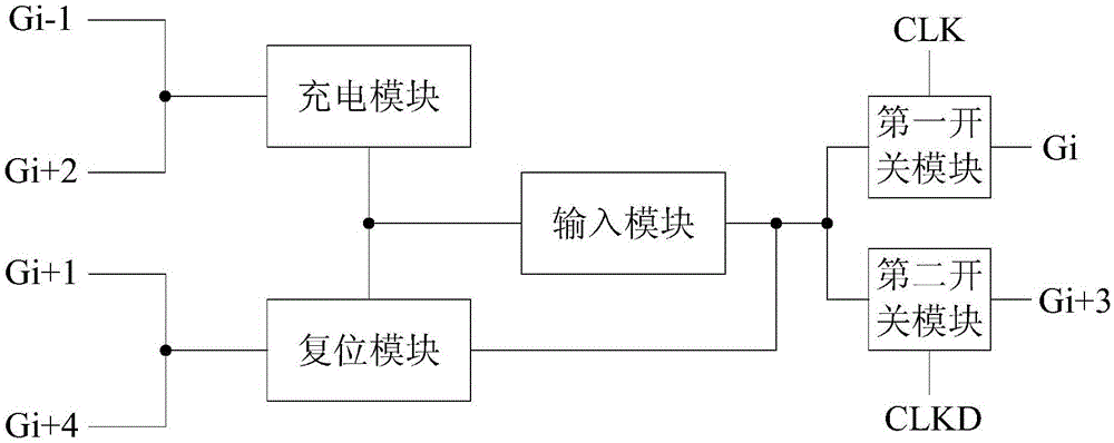
[0051] Such as figure 1 As shown, the shift register unit includes an input module, a charging module, a reset module, a first switch module and a second switch module.
[0052] The output terminal of the input module is connected to the i-th gate line Gi through the first switch module, and connected to the i+3-th gate line Gi+3 through the second switch module. The control end of the first switch module is connected to the first clock signal line, the control end of the second switch module is connected to the second clock signal line, and the phase difference between the first clock signal line and the second clock signal line is half a period, combined figure 2 As shown, in this embodiment, CLK is connected to the control terminal of the first switch module, and CLKD is connected to the control terminal of the second switch module.
[0053] The i-1th grid line Gi-1 and the i+2th grid line Gi+2 are connected to the input terminal of the input module through the charging m...
Embodiment 2
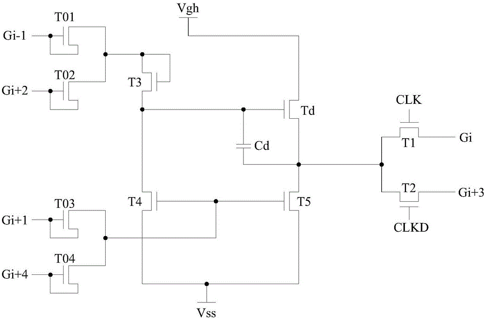
[0059] This embodiment is a more specific implementation on the basis of Embodiment 1, such as image 3 As shown, in this embodiment, the input module includes a capacitor Cd and an output switch Td, the two ends of Cd are respectively connected to the gate and drain of Td, and the source of Td is connected to the high-level signal line Vgh. The gate of Td (the first terminal of Cd) is used as the input terminal of the input module, and the drain of Td (the second terminal of Cd) is used as the output terminal of the input module. In this embodiment, all the switch transistors are preferably thin film transistors (ThinFilmTransistor, TFT for short).
[0060] Such as image 3 As shown, as a preferred solution, the charging module includes a third switching tube T3. Gi-1 and Gi+2 are connected to the gate and source of T3, and the drain of T3 is connected to the input terminal of the input module, that is, the gate of Td (the first terminal of Cd).
[0061] When Gi-1 or Gi+2 ...
Embodiment 3
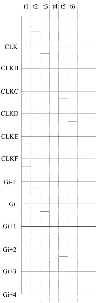
[0071] Such as Figure 5 As shown, the embodiment of the present invention provides a GOA circuit, including n gate lines, six clock signal lines that cyclically output high-level pulse signals, and several shift register units provided in Embodiment 1 and Embodiment 2.
[0072] Such as Figure 5 As shown, the gate of T1 in the j-th shift register unit is connected to CLK, the gate of T1 in the j+1-th shift register unit is connected to CLKB, and the gate of T1 in the j+2-th shift register unit The gate is connected to CLKC, the gate of T2 in the jth shift register unit is connected to CLKD, the gate of T2 in the j+1 shift register unit is connected to CLKE, and the gate of T2 in the j+2 shift register unit The gate of T2 is connected to CLKF.
[0073]Gi is connected to the drain of T1 in the shift register unit of the jth stage, and the shift register unit of the next stage, that is, the charging module in the shift register unit of the j+1st stage. In addition, if Gi is n...
PUM
 Abstract
Description
Claims
Application Information
 - R&D
- Intellectual Property
- Life Sciences
- Materials
- Tech Scout
- Unparalleled Data Quality
- Higher Quality Content
- 60% Fewer Hallucinations
Browse by: Latest US Patents, China's latest patents, Technical Efficacy Thesaurus, Application Domain, Technology Topic, Popular Technical Reports.
© 2025 PatSnap. All rights reserved.Legal|Privacy policy|Modern Slavery Act Transparency Statement|Sitemap|About US| Contact US: help@patsnap.com