Solid-state imaging device and switching circuit

A technology of solid-state imaging device and amplifying circuit, which is applied to circuits, electric solid-state devices, radiation control devices, etc., can solve the problem of random noise becoming larger, and achieve the effect of reducing noise.

Inactive Publication Date: 2017-08-25
PANASONIC INTELLECTUAL PROPERTY MANAGEMENT CO LTD
View PDF1 Cites 0 Cited by
  • Summary
  • Abstract
  • Description
  • Claims
  • Application Information

AI Technical Summary

Problems solved by technology

Therefore, in the solid-state imaging device disclosed in Patent Document 1, there is a problem that random noise becomes large.

Method used


Image

  • Solid-state imaging device and switching circuit
  • Solid-state imaging device and switching circuit
  • Solid-state imaging device and switching circuit

Examples


no. 1 Embodiment approach )

[0062] Hereinafter, a first embodiment of the present invention will be described with reference to the drawings. Here, the same symbols are assigned to the same elements as those already described, and description thereof may be omitted. In the following, the transistor is assumed to be an n-type MOS, but a p-type MOS can also perform the same operation. In addition, what is described below as the source / drain of a transistor means either the source or the drain (in an actual device, the source and the drain are the same thing and cannot be distinguished). However, when one of them is given a higher voltage than the other, it is called a drain.

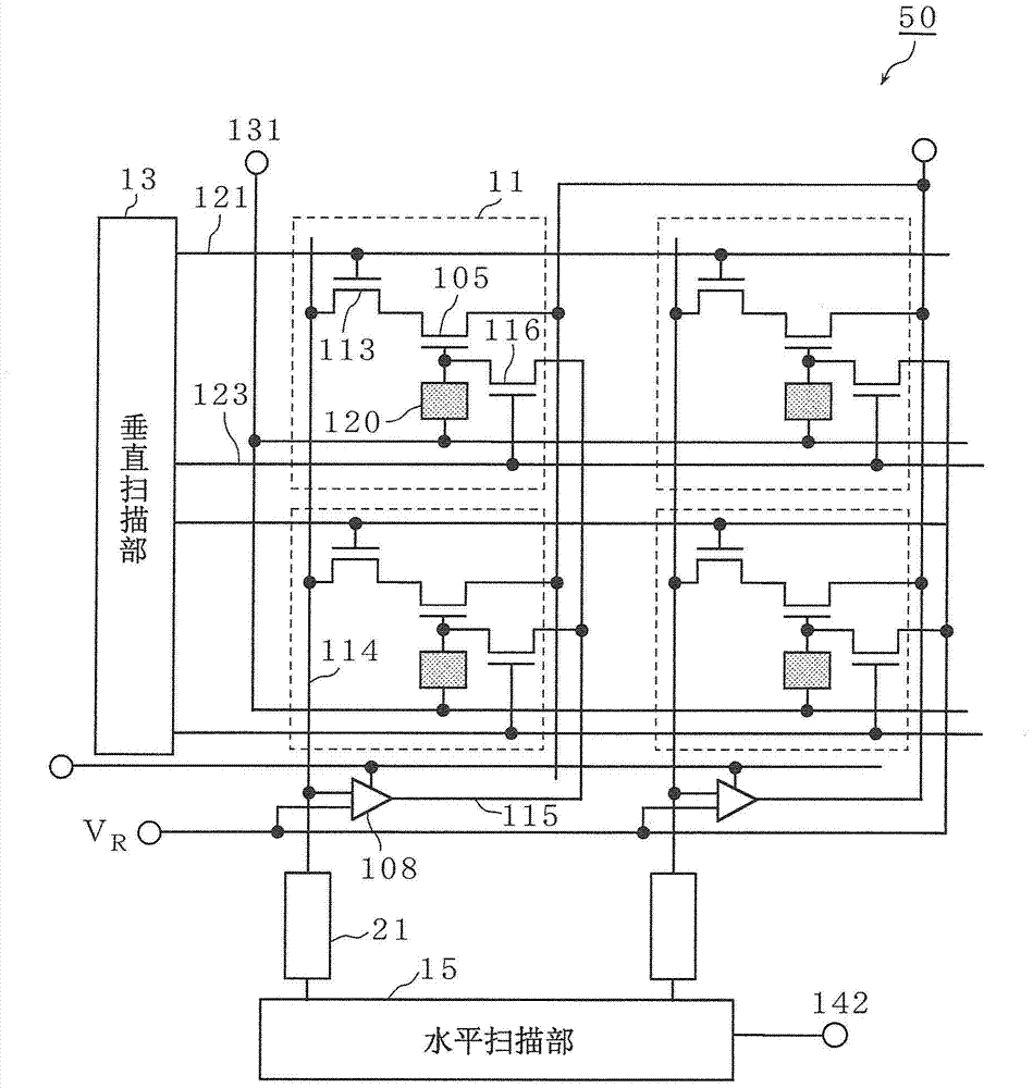
[0063] First, the configuration of the solid-state imaging device according to the first embodiment of the present invention will be described.

[0064] Figure 5 It is a circuit diagram of the solid-state imaging device 200 according to the first embodiment of the present invention. exist Figure 5 In , in order to simplify the...

no. 2 Embodiment approach )

[0133] Hereinafter, a second embodiment of the present invention will be described with reference to the drawings. Here, differences from the first embodiment will be mainly described, and descriptions of overlapping parts will be omitted.

[0134] Figure 8 It is a circuit diagram of the solid-state imaging device 300 according to the second embodiment of the present invention.

[0135] Figure 8 The solid-state imaging device 300 shown is different from Figure 5 The illustrated solid-state imaging device 200 is characterized in that the output terminal of the second amplifier circuit 206 is connected to the source of the amplifier transistor 105 . That is, the pixel sharing circuit 311 does not have Figure 5 The capacitive element 204 is shown. In addition, the solid-state imaging device 300 further includes a switch 317 and a power supply line 318 .

[0136] Specifically, the output terminal of the second amplifier circuit 206 is connected to the drain of the amplif...

no. 3 Embodiment approach )

[0145] Hereinafter, a third embodiment of the present invention will be described with reference to the drawings. Hereinafter, differences from the first embodiment will be mainly described, and overlapping descriptions will be omitted.

[0146] Figure 9 It is a circuit diagram of the solid-state imaging device 400 according to the third embodiment of the present invention.

[0147] Figure 9 The solid-state imaging device 400 shown is different from Figure 5 The illustrated solid-state imaging device 200 is characterized in that the output terminal of the second amplifier circuit 206 is connected to the node of the transfer transistor 101 on the photoelectric conversion unit 120 side through the capacitive element 404 .

[0148] Specifically, the pixels 410 ( 410 a and 410 b ) further include capacitive elements 404 ( 404 a and 404 b ). The output terminal of the second amplifier circuit 206 is connected to one end of the capacitive element 404 through the switch 207 . T...


PUM


Abstract

A solid-state imaging device (200) according to an aspect of the present invention includes: a photoelectric conversion unit (12) that converts light into signal charges; a storage unit (230) that stores the signal charges; Between the parts (230), the above-mentioned signal charge converted by the photoelectric conversion part (120) is transferred to the transfer transistor (101) of the storage part (230); the gate is connected to the storage part (230), and the storage part (230) The amplifying transistor (105) that amplifies the signal charge accumulated in the amplifier to generate a voltage signal; the reset transistor (116) that resets the voltage of the storage part (230); negatively feeds back the above-mentioned voltage signal generated by the amplifying transistor (105) to the reset The first amplifier circuit (108) of the transistor (116); positively feeds back the above-mentioned voltage signal generated by the amplifier transistor (105) to the second amplifier circuit (206) of the amplifier transistor (105).

Description

technical field [0001] The present invention relates to a solid-state imaging device and a switch circuit. Background technique [0002] In a general solid-state imaging device, an embedded photodiode is used as a photoelectric conversion unit. [0003] In addition, Patent Document 1 discloses a multilayer solid-state imaging device. In this multilayer solid-state imaging device, a photoelectric conversion film is formed on the control electrode, and a transparent electrode layer is formed on the photoelectric conversion film. The multilayer solid-state imaging device transmits the voltage applied to the transparent electrode to the control electrode through the action of the photoelectric conversion film, thereby converting optical information into an electrical signal with a good signal-to-noise ratio. [0004] A multilayer solid-state imaging device has a structure in which a photoelectric conversion film is formed on a semiconductor substrate on which a pixel circuit i...

Claims


Application Information

Patent Timeline
Patent Type & Authority Patents(China)
IPC IPC(8): H04N5/374H01L27/146H04N5/363
CPCH01L27/14665H01L27/14692H04N25/65H01L27/14601
Inventor 石井基范春日繁孝
Owner PANASONIC INTELLECTUAL PROPERTY MANAGEMENT CO LTD
Why Eureka
Try Eureka