solid state imaging device

A solid-state imaging device and pixel technology, applied in electric solid-state devices, radiation control devices, image communication, etc., to achieve the effect of reducing kTC noise

Active Publication Date: 2017-07-28
PANASONIC INTELLECTUAL PROPERTY MANAGEMENT CO LTD
View PDF2 Cites 0 Cited by
  • Summary
  • Abstract
  • Description
  • Claims
  • Application Information

AI Technical Summary

Problems solved by technology

[0010] The technology disclosed in Patent Document 2 such as Figure 14 As shown, the unit pixel 510 can only be adapted to the case of having four transistors of the amplification transistor 514, the reset transistor 516, the row selection transistor 518, and the transistor 520.

Method used


Image

  • solid state imaging device
  • solid state imaging device
  • solid state imaging device

Examples


Embodiment Construction

[0028] Hereinafter, a solid-state imaging device and a driving method according to an embodiment will be described with reference to the drawings. Furthermore, although the solid-state imaging device according to the present invention will be described using the following embodiments and drawings, these are merely examples, and the solid-state imaging device according to the present invention is not limited to these examples.

[0029] (first embodiment)

[0030] The overall configuration of the solid-state imaging device according to the first embodiment will be described.

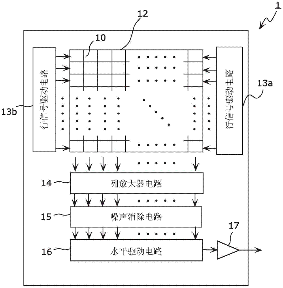
[0031] figure 1 It is a block diagram showing the overall configuration of the solid-state imaging device according to the embodiment. The solid-state imaging device 1 described in this figure includes: a pixel unit 12 in which a plurality of pixels 10 are arranged in a matrix; row signal drive circuits 13a and 13b; a column amplifier circuit 14 composed of amplifier circuits arranged for each column; ...


PUM


Abstract

The pixel (10) includes: a photoelectric conversion unit (21); a charge accumulation unit (115); an amplification transistor (116) whose gate is connected to the charge accumulation unit (115); a source connected to the source of the amplification transistor (116), a select transistor (202) whose drain is connected to the column signal line (23); and a reset transistor (117) whose source is connected to the charge accumulation part (115) and whose drain is connected to the column signal line (23); During the output period, the first voltage that makes the selection transistor (202) into a conductive state is applied to the gate of the selection transistor (202), and the second voltage that makes the reset transistor (117) into a non-conductive state is applied to the reset transistor ( 117), the intermediate voltage between the first voltage and the second voltage is applied to the gate of the selection transistor (202) during the reset period of the charge accumulation unit (115).

Description

technical field [0001] The present invention relates to a solid-state imaging device, and more particularly to a stacked solid-state imaging device. Background technique [0002] Patent Document 1 discloses a stacked solid-state imaging device. In the multilayer solid-state imaging device disclosed in Patent Document 1, noise occurs when signal charges are reset. Specifically, when the pulse shape of the reset pulse is steep when it is turned off, kTC noise occurs because the charge on the channel moves to either the source or the drain of the reset transistor is random. In addition, kTC noise is also generated due to capacitive coupling between the reset signal line and the pixel electrode or the like. [0003] Furthermore, even if correlated double sampling is used in a stacked solid-state imaging device, kTC noise cannot be completely eliminated. This is because, in a stacked solid-state imaging device, the photoelectric conversion unit provided above the semiconductor...

Claims


Application Information

Patent Timeline
Patent Type & Authority Patents(China)
IPC IPC(8): H01L27/146H04N5/363H04N5/374
CPCH01L27/14609H01L27/14621H01L27/14627H04N25/709H04N25/70H04N25/75H10K39/32H04N25/745
Inventor 石井基范
Owner PANASONIC INTELLECTUAL PROPERTY MANAGEMENT CO LTD
Why Eureka
Try Eureka