Solid-state imaging device and driving method thereof

A solid-state imaging device and pixel technology, which is applied to static cameras, electric solid-state devices, radiation control devices, etc., to reduce kTC noise, increase inter-pixel interference, and reduce parasitic capacitance.

Active Publication Date: 2017-06-27
PANASONIC INTELLECTUAL PROPERTY MANAGEMENT CO LTD
View PDF1 Cites 0 Cited by
  • Summary
  • Abstract
  • Description
  • Claims
  • Application Information

AI Technical Summary

Problems solved by technology

The reason for this is that there must be a wiring or contact of a conductor between the photoelectric conversion part and the floating diffusion, and it is impossible to completely transfer a large amount of charge in the conductor.

Method used


Image

  • Solid-state imaging device and driving method thereof
  • Solid-state imaging device and driving method thereof
  • Solid-state imaging device and driving method thereof

Examples


Embodiment approach 1

[0098] Hereinafter, Embodiment 1 in the present invention will be described with reference to the drawings. Parts given the same number represent the same location. Hereinafter, the transistor is assumed to be an n-type MOS, but it goes without saying that it can also operate in the same way in the case of a p-type MOS. In addition, below, when describing as a source and a drain of a transistor, it means either a source or a drain (this is because a source and a drain are completely the same and cannot be distinguished in an actual element). However, when the voltage applied to one of them is higher than that of the other, it is marked as a drain.

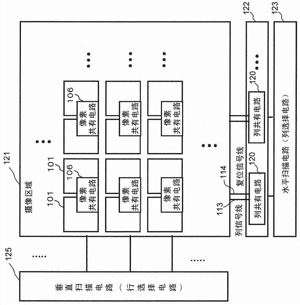
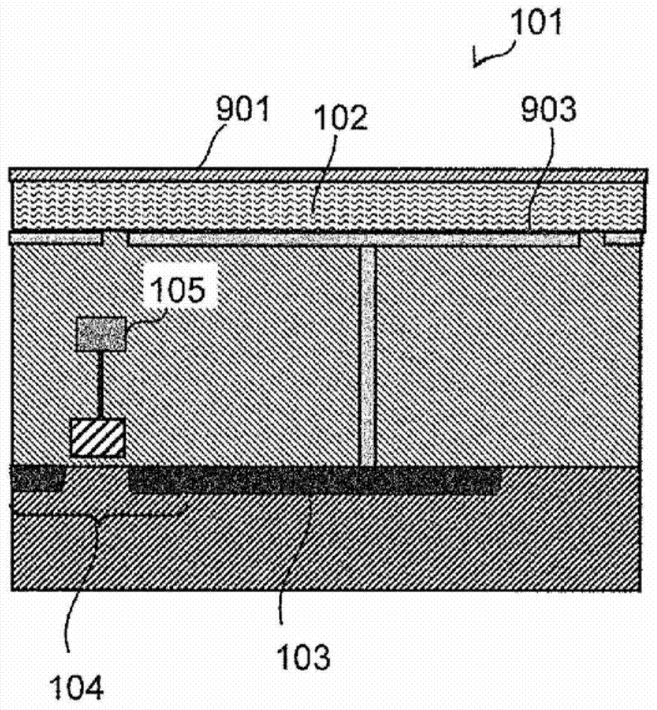
[0099] Figure 1A It is a block diagram showing the configuration of the solid-state imaging device in Embodiment 1 of the present invention. The solid-state imaging device in the figure includes an imaging region 121 , a vertical scanning circuit (row selection circuit) 125 , a column processing circuit 122 , and a horizontal s...

Embodiment approach 2

[0170] Hereinafter, Embodiment 2 in the present invention will be described with reference to the drawings. Parts given the same number represent the same location. Hereinafter, the transistor is assumed to be an n-type MOS, but it goes without saying that it can also operate in the same way in the case of a p-type MOS. In addition, below, when describing as a source and a drain of a transistor, it means either a source or a drain (this is because a source and a drain are completely the same and cannot be distinguished in an actual element). However, when the voltage applied to one of them is higher than that of the other, it is marked as a drain.

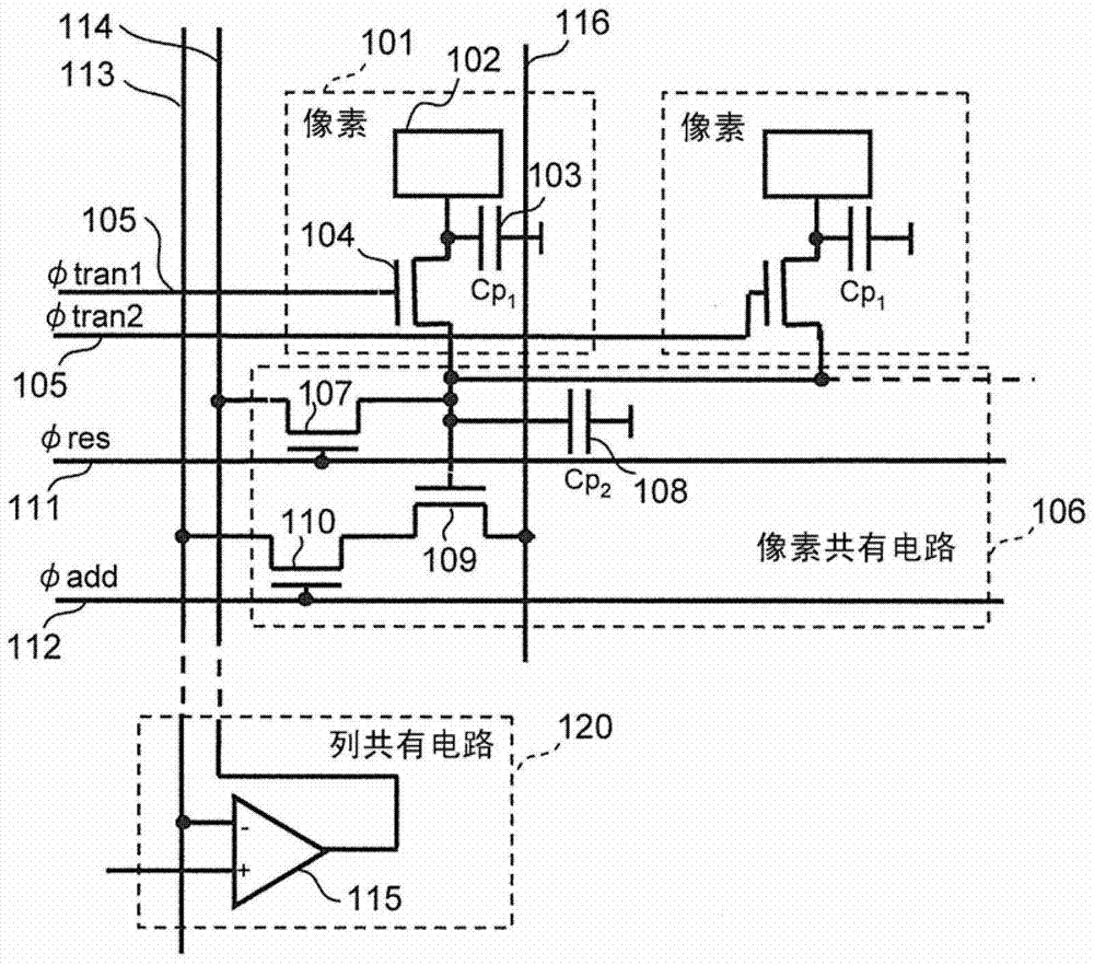
[0171] In Embodiment 2 of the present invention, the circuit diagram is also Figure 1B same. The difference lies in the driving method. image 3 A driving method in Embodiment 2 of the present invention is shown. Each symbol is the same as that of Embodiment 1. image 3 Main concern Figure 1B The illustrated plurality of p...

Embodiment approach 3

[0190] A driving method of the solid-state imaging device in Embodiment 3 of the present invention will be described with reference to the drawings.

[0191] In Embodiment 1, when reading the reset voltage into the CDS circuit, φtran is turned off. On the other hand, φtran is turned on when the signal voltage is read out. Therefore, the reading of the signal voltage is affected by the parasitic capacitance of the connection transistor 104 . That is, when the difference between the conduction voltage of φtran and the threshold voltage of the connection transistor 104 is ΔV, and the parasitic capacitance is Cc, the voltage of Equation 10 is superimposed on the signal voltage.

[0192] 【Number 12】

[0193] (Formula 10)

[0194] This voltage ΔV depends on the threshold voltage of the connection transistor 104 . Also, the threshold voltage of the connection transistor 104 usually varies among the individual pixels 101, and fixed pattern noise reflecting the variation is super...


PUM


Abstract

The solid-state imaging device of the present invention includes: a plurality of pixels (101) arranged in a two-dimensional shape; a plurality of pixel sharing circuits (106) shared by a certain number of adjacent pixels, and one is arranged for each certain number of pixels , arranged in a matrix; the column sharing circuit (120), one for each column of a plurality of pixel sharing circuits (106), shared by the pixel sharing circuits (106) belonging to the same column; the column signal line (113), according to Each column of the pixel common circuit (106) is configured; and the reset signal line (114) is configured according to each column of the pixel common circuit (106); the respective electrical signals of multiple pixels are detected by the pixel common circuit (106), and transmitted through the column The signal line (113) is read out to the column sharing circuit (120), and the electrical signal detected by the pixel sharing circuit (106) passes through the The feedback path is reset.

Description

technical field [0001] The present invention relates to solid-state imaging devices and the like, and relates to solid-state imaging devices and the like used in electronic still cameras, surveillance cameras, video cameras, and the like. Background technique [0002] A solid-state imaging device is generally called an image sensor or the like, and its type is roughly classified into a CCD sensor or a MOS sensor. In these solid-state imaging devices in which photodiodes are formed on silicon substrates, there are three disadvantages, especially in the case of miniaturization of pixels. [0003] (Material) The first one is that the photodiode has a performance limit due to the material characteristics of silicon, so the sensitivity is reduced. For example, when light with a wavelength of 550 nm, which is green light, is incident on silicon at 2 μm, only about 92% is absorbed. In other words, even if a photodiode with a depth of 2 μm is formed, it is impossible to obtain the...

Claims


Application Information

Patent Timeline
Patent Type & Authority Patents(China)
IPC IPC(8): H04N5/363H01L27/146H04N5/3745H04N5/376H04N101/00
CPCH01L27/1461H01L27/1464H04N25/65H04N25/778H04N25/75
Inventor 石井基范春日繁孝森三佳
Owner PANASONIC INTELLECTUAL PROPERTY MANAGEMENT CO LTD
Why Eureka
Try Eureka