Supercharge Your Innovation With Domain-Expert AI Agents!

Electronic component mounting system and electronic component mounting method

A technology for electronic component installation and electronic components, which is applied in the direction of electrical components, electrical components, etc., can solve problems such as insufficient joint strength, interference, and the height of shielding components cannot be consistent with the specified size, and achieve sufficient joint strength and accurate height dimensions.

Active Publication Date: 2017-10-13
PANASONIC INTELLECTUAL PROPERTY MANAGEMENT CO LTD
View PDF2 Cites 0 Cited by
  • Summary
  • Abstract
  • Description
  • Claims
  • Application Information

AI Technical Summary

Problems solved by technology

Such a gap occurs when the shielding element is mounted with a foreign object such as a dropped component remaining on the shielding electrode. If the solder joint is completed with the gap generated, the height of the shielding element cannot match the mounting surface of the completed substrate. The specified dimensions are the same, and there is a problem that interference with other parts occurs when the substrate is mounted on the case
Therefore, such troubles are increasing in frequency with the size reduction and thinning of electronic devices such as mobile devices, and effective countermeasures are required.
In addition, the solder supplied to the shielding electrode by screen printing cannot always ensure an appropriate amount due to printing deviations, etc., and there is a problem that a sound solder joint cannot be formed at the site where "flash" occurs in the screen printing. Situations that result in insufficient joint strength

Method used


Image

  • Electronic component mounting system and electronic component mounting method
  • Electronic component mounting system and electronic component mounting method
  • Electronic component mounting system and electronic component mounting method

Examples


Embodiment Construction

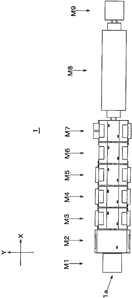
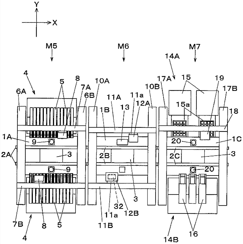
[0038] Hereinafter, embodiments of the present invention will be described with reference to the drawings. First, refer to figure 1 , figure 2 , the structure of the electronic component mounting system 1 will be described. exist figure 1 Among them, the electronic component mounting system 1 has the following function: using the electronic component mounting line 1a composed of a plurality of equipment (substrate supply device M1 to substrate recovery device M9) having a conveying member for conveying substrates, electronic components and substrates for covering A shield element of the electronic component mounted on the substrate is mounted on the substrate. in addition, figure 2 The detailed structure of the 1st electronic component mounting apparatus M5, the solder coating apparatus M6, and the 2nd electronic component mounting apparatus M7 is shown.

[0039] The electronic component mounting production line 1a connects the substrate supply device M1, the solder pri...


PUM


Abstract

The present invention provides an electronic component mounting system and an electronic component mounting method capable of mounting shielding components with accurate height dimensions and sufficient bonding strength. An inspection process is provided, after the electronic component (21) is mounted on the first solder part (S1) for electronic component bonding and before the shielding component (22) is mounted on the second solder part (S2) for shielding component bonding, the inspection The area (23) where the wall portion of the mounted shielding element (22) is located is free of foreign matter, and the substrate ( 3) The area (23) is coated with solder to form the additional solder portion (SA) and then the shielding element (22) is mounted to set the work process. As a result, soldering is prevented from being performed in a state where foreign objects are interposed and an inappropriate amount of solder is used, and the shielding element ( 22 ) can be mounted with an accurate height dimension and sufficient bonding strength.

Description

technical field [0001] The present invention relates to an electronic component mounting system and an electronic component mounting method for manufacturing a mounting substrate by mounting an electronic component on a substrate. Background technique [0002] An electronic component mounting system that mounts electronic components on a substrate to manufacture a mounted substrate is mainly composed of an electronic component mounting line that connects a plurality of component mounting equipment such as a solder printing device and an electronic component mounting device. The substrate is conveyed from the upstream side to the downstream side on the electronic component mounting line, and components mounting operations such as solder printing and component mounting are performed sequentially on the substrate. Here, when electromagnetic shielding is required on a mounting substrate to be produced, a shielding element is mounted on the mounting surface of the substrate so as...

Claims


Application Information

Patent Timeline
Patent Type & Authority Patents(China)
IPC IPC(8): H05K13/04
Inventor 山本邦雄冈本健二石本宪一郎冈村浩志
Owner PANASONIC INTELLECTUAL PROPERTY MANAGEMENT CO LTD
Features
  • R&D
  • Intellectual Property
  • Life Sciences
  • Materials
  • Tech Scout
  • Unparalleled Data Quality
  • Higher Quality Content
  • 60% Fewer Hallucinations
Learn More