
led light source array projection test device

An LED light source and testing device technology, applied in the field of lighting and display, can solve the problems of higher packaging process requirements, difficult operation of the testing method, and high integration, and achieves simple and flexible installation and disassembly, convenient and fast testing process, and simple device structure. Effect

Active Publication Date: 2016-07-27
INST OF SEMICONDUCTORS - CHINESE ACAD OF SCI
View PDF5 Cites 0 Cited by
  • Summary
  • Abstract
  • Description
  • Claims
  • Application Information

AI Technical Summary

Problems solved by technology

[0005] However, whether it is a high-power-density LED lighting source or a high-definition small-pitch LED display, its characteristics are that the size of the LED chip is small and the integration is high, so the requirements for the packaging process are higher.
Since the current LED integrated packaging mainly relies on gold wire connection, there are still some shortcomings in the yield of high-density LED products.
At the same time, these two types of high-density LED products have high brightness when they are turned on. It is impossible to observe the number and location of dead pixels with eyes.
This leads to the inability to perform simple manual screening of products at the initial stage, thereby increasing equipment costs and product production and delivery time
[0006] The existing LED light source array test device has a complex structure, high cost, and the test method is not easy to operate. Therefore, it is an urgent problem for practitioners in the field to find a device that has a simple structure and can accurately find fault points in the LED light source array.

Method used


Image

  • led light source array projection test device
  • led light source array projection test device
  • led light source array projection test device

Examples


Embodiment Construction

[0044] In order to make the object, technical solution and advantages of the present invention clearer, the present invention will be described in further detail below in conjunction with specific embodiments and with reference to the accompanying drawings. It should be noted that, in the drawings or descriptions of the specification, similar or identical parts all use the same figure numbers. Implementations not shown or described in the accompanying drawings are forms known to those of ordinary skill in the art. Additionally, while illustrations of parameters including particular values ​​may be provided herein, it should be understood that the parameters need not be exactly equal to the corresponding values, but rather may approximate the corresponding values ​​within acceptable error margins or design constraints. The directional terms mentioned in the embodiments, such as "upper", "lower", "front", "rear", "left", "right", etc., are only referring to the directions of the...


PUM


Abstract

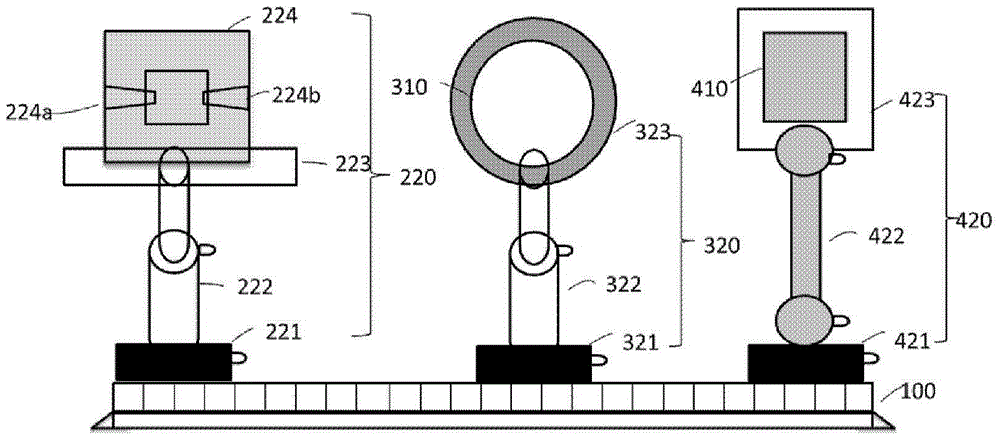
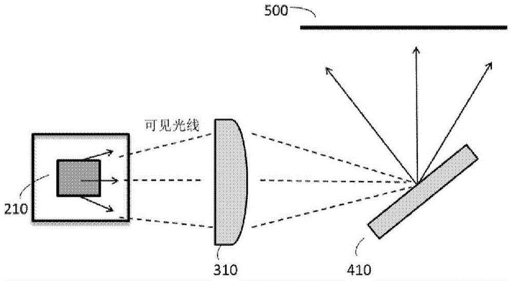
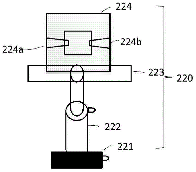
The invention provides an LED (Light-Emitting Diode) light source array projection testing device. The LED light source array projection testing device comprises a beam-expanding element which is positioned at the back end of the light path of a tested LED light source array, a projection element positioned at the back end of the light path of the beam-expanding element, and a projection surface positioned at the back end of the light path of the projection element, wherein light beams emitted by the tested LED light source array are projected onto the projection surface through the projection element after being expanded by the beam-expanding element; a single LED light source in the tested LED light source array corresponds to a position on the projection surface. According to the LED light source array projection testing device, a light source matrix module can be presented on any plane in a similar projection way by using a lens and a reflecting mirror, and a fault point can be found by means of visual inspection. The device is simple in structure, convenient and rapid in the testing process, and low in cost.

Description

technical field [0001] The invention relates to the field of illumination and display, in particular to an LED light source array projection test device. Background technique [0002] Today, when advocating energy-saving, environmentally friendly and low-carbon life, light-emitting diodes (LEDs) are more and more widely used in the fields of lighting, display and communication. As a result, the demand for high-power-density LED lighting sources and high-density small-pitch LED displays continues to increase. [0003] High power density LED lighting source is a new packaging form of small size and high power LED derived to meet the market demand for high power lighting source. Its appearance solves the shortcomings of large size and high cost of high-power light sources. Due to its high integration and low cost, it will become an inevitable trend in the development of high-power lighting sources for indoor and outdoor and special occasions. [0004] Similarly, the high-defi...

Claims


Application Information

Patent Timeline
Patent Type & Authority Patents(China)
IPC IPC(8): G01M11/02
Inventor 裴艳荣杨华刘立莉李璟王军喜李晋闽
Owner INST OF SEMICONDUCTORS - CHINESE ACAD OF SCI
Learn More