Array substrate, display panel and display device

An array substrate and substrate technology, which is applied in the field of display panels and display devices, can solve problems such as horizontal horizontal stripes, and achieve the effects of reducing horizontal stripes, improving display effect, and reducing parasitic capacitance.

Active Publication Date: 2016-09-07
SHANGHAI AVIC OPTOELECTRONICS +1
View PDF5 Cites 0 Cited by
  • Summary
  • Abstract
  • Description
  • Claims
  • Application Information

AI Technical Summary

Problems solved by technology

[0005] The object of the present invention is to provide an array substrate, a display panel and a display device to solve the problem of horizontal stripes in the image display process

Method used


Image

  • Array substrate, display panel and display device
  • Array substrate, display panel and display device
  • Array substrate, display panel and display device

Examples


Embodiment Construction

[0022] The implementation process of the embodiment of the present invention will be described in detail below in conjunction with the accompanying drawings. It should be noted that the same or similar reference numerals represent the same or similar elements or elements having the same or similar functions throughout. The embodiments described below by referring to the figures are exemplary only for explaining the present invention and should not be construed as limiting the present invention.

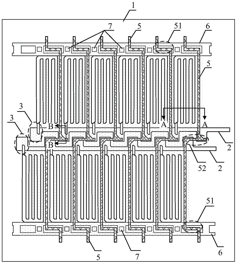
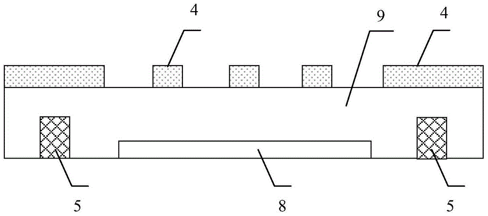
[0023] see figure 2 , the embodiment of the present invention provides an array substrate, including a substrate 1 , a gate line 2 formed on the substrate 1 and an array of sub-pixel units, each sub-pixel unit including a TFT 3 . see image 3 ,show figure 2 The schematic cross-sectional view of the array substrate shown at AA, each sub-pixel unit also includes a pixel electrode 8 and a common electrode 4, and the common electrode 4 is a comb-shaped structure (usually, including a...


PUM


Abstract

The invention discloses an array substrate with an aim to solve the problem about horizontal cross grains in the process of image displaying. The array substrate comprises a substrate, grid lines and a sub-pixel unit array, wherein the grid lines and the sub-pixel unit array are formed on the substrate. Each sub-pixel unit comprises a TFT (thin film transistor) and a public electrode, every two adjacent rows of sub-pixel units constitute a sub-pixel unit group, and two grid lines are arranged between the two rows of sub-pixel units of the sub-pixel unit group; gate electrodes of the TFTs of the last row of sub-pixel units in the sub-pixel unit group and gate electrodes of the TFTs of the next row of sub-pixel units are arranged between the two grid lines and staggered, the gate electrodes of the TFTs are arranged on the same sides of respective sub-pixel units, and the two rows of sub-pixel units of the sub-pixel unit groups are staggered by the width smaller than one sub-pixel unit along the direction of the grid lines. The invention further discloses a display panel and a display device.

Description

technical field [0001] The present invention relates to the display field, in particular to an array substrate, a display panel and a display device including the array substrate. Background technique [0002] Thin Film Transistor-Liquid Crystal Display (TFT-LCD) includes an array substrate, a color filter substrate and a liquid crystal layer between them. In order to achieve a better display effect, a high aperture ratio is the goal pursued by every manufacturer. [0003] see figure 1 , is a high aperture ratio array substrate. Including cross-arranged gate lines 101 and data lines 102, common electrode lines 103, and sub-pixel units surrounded by data lines 102 and gate lines 101 ( figure 1 Only the upper and lower sub-pixel units in two adjacent columns of sub-pixel units are shown), each sub-pixel unit includes a TFT 104 and a pixel electrode 105; two adjacent rows of gate lines 101 are located between two adjacent rows of sub-pixel units Between two adjacent rows of...

Claims


Application Information

Patent Timeline
Patent Type & Authority Patents(China)
IPC IPC(8): G02F1/1362G02F1/1368H01L29/786H01L29/423
Inventor 刘波简守甫席克瑞
Owner SHANGHAI AVIC OPTOELECTRONICS
Why Eureka
Try Eureka