Array substrate, manufacturing method, and display device

A technology for array substrates and manufacturing methods, which is applied in semiconductor/solid-state device manufacturing, semiconductor/solid-state device components, instruments, etc., and can solve problems such as large distance differences, horizontal stripes on display, and different signal transmission delay times

Pending Publication Date: 2017-12-29
BOE TECH GRP CO LTD +1
View PDF5 Cites 11 Cited by
  • Summary
  • Abstract
  • Description
  • Claims
  • Application Information

AI Technical Summary

Problems solved by technology

[0008] Embodiments of the present invention provide an array substrate, a manufacturing method thereof, and a display device, which can solve the problem in the prior art that the distance between the shielding layer and the lead of the first signal line and the distance between the lead of the second signal line are relatively large. The signal transmission delay time is different due to the large size, which will cause horizontal stripes in the display

Method used


Image

  • Array substrate, manufacturing method, and display device
  • Array substrate, manufacturing method, and display device
  • Array substrate, manufacturing method, and display device

Examples


Embodiment Construction

[0041] The following will clearly and completely describe the technical solutions in the embodiments of the present invention with reference to the accompanying drawings in the embodiments of the present invention. Obviously, the described embodiments are only some, not all, embodiments of the present invention. Based on the embodiments of the present invention, all other embodiments obtained by persons of ordinary skill in the art without making creative efforts belong to the protection scope of the present invention.

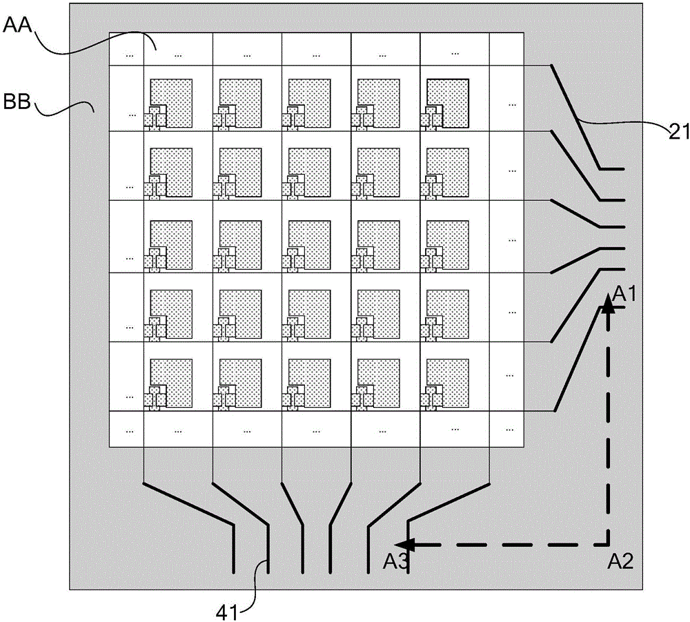
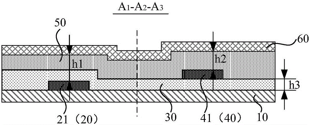
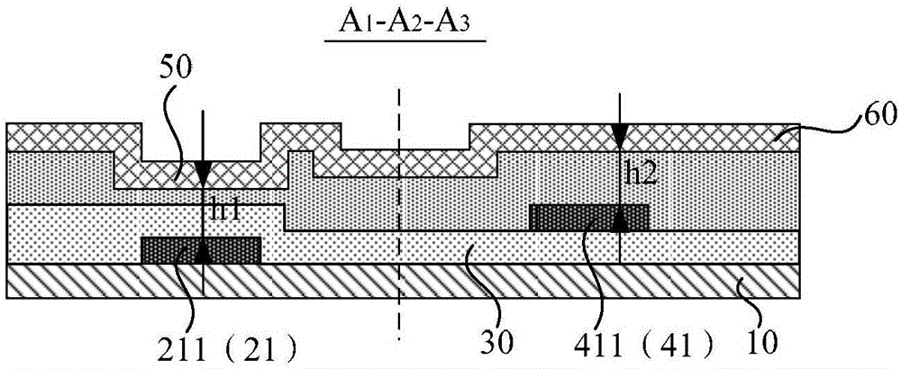
[0042]An embodiment of the present invention provides an array substrate, such as figure 1 As shown, including the display area AA and the wiring area BB outside the display area, such as figure 2 As shown, the array substrate includes a base substrate 10, on which a first conductive layer 20, a first insulating layer 30, a second conductive layer 40, a second insulating layer 50 and a shield located in the routing area BB are sequentially arranged. Layer 60...


PUM


Abstract

The embodiment of the invention provides an array substrate, a manufacturing method and a display device, and relates to the technical field of display. The method can solve problems that the signal transmission delay time is different because the bigger difference of the distance between a shielding layer and a first signal line lead wire and the distance between the shielding layer and a second signal line lead wire, and thereby lateral stripes are generated in display. The array substrate comprises a display region and a wiring region outside the display region. The array substrate comprises a substrate, and the substrate is sequentially provided with a first conductive layer, a first insulating layer, a second conductive layer, a second insulating layer and a shielding layer located in the wiring region. The first conductive layer comprises a first signal line lead wire of the wiring region, and the second conductive layer comprises a second signal line lead wire of the wiring region. The orthographic projections of the first and second signal line lead wires are not overlapped. The difference between the vertical distance from the first signal line lead wire to the shielding layer and the vertical distance from the second signal line lead wire to the shielding layer is less than the thickness of the first insulating layer.

Description

technical field [0001] The present invention relates to the field of display technology, in particular to an array substrate, a manufacturing method thereof, and a display device. Background technique [0002] Thin Film Transistor Liquid Crystal Display (TFT-LCD for short) usually includes an array substrate, a color filter substrate and a liquid crystal layer between them; wherein, the display area of ​​the array substrate includes a plurality of horizontal and vertical grid lines The sub-pixels defined by the data lines, the grid lines and data lines that cross vertically and vertically in the display area are respectively drawn out through the gate signal line leads and the data signal line leads in the fan-out (Fanout) area and connected to the integrated circuit chip (Integrated Circuit, IC) bind connection. [0003] At the moment when the display is turned on, the electrical signal passing through the gate line will change sharply, so that a large amount of induced ch...

Claims


Application Information

Patent Timeline
Patent Type & Authority Applications(China)
IPC IPC(8): H01L23/58H01L27/12H01L21/84
CPCH01L23/585H01L27/124H01L27/1259G02F1/136209G02F1/133388G02F1/136277G02F1/133512H01L27/127G02F1/136286
Inventor 徐元杰高山
Owner BOE TECH GRP CO LTD
Why Eureka
Try Eureka