Array substrate, manufacturing method thereof and liquid crystal display component

A technology of an array substrate and a manufacturing method, which is applied in the field of liquid crystal display, can solve the problems of difficult rotation of liquid crystal molecules, uneven pressing, disclination and uneven pressing, and achieves the effect of improving the disclination and uneven pressing.

Active Publication Date: 2014-08-13
XIAMEN TIANMA MICRO ELECTRONICS +1
View PDF6 Cites 6 Cited by
  • Summary
  • Abstract
  • Description
  • Claims
  • Application Information

AI Technical Summary

Problems solved by technology

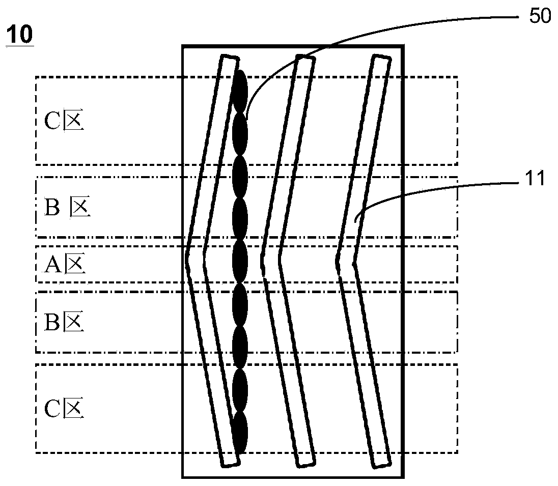
[0007] At the same time, since the liquid crystal molecules in the A region and the B region are difficult to rotate, once the liquid crystal molecules are pressed, it is difficult to recover, so the uneven pressing (trace mura) occurs.
[0008] Therefore, how to solve the disclination and uneven pressing phenomenon existing in the existing IPS mode and FFS mode liquid crystal display devices has become a technical problem to be solved urgently by those skilled in the art.

Method used


Image

  • Array substrate, manufacturing method thereof and liquid crystal display component
  • Array substrate, manufacturing method thereof and liquid crystal display component
  • Array substrate, manufacturing method thereof and liquid crystal display component

Examples


Embodiment Construction

[0030] An array substrate, a manufacturing method thereof, and a liquid crystal display device provided by the present invention will be further described in detail below with reference to the accompanying drawings and specific embodiments. Advantages and features of the present invention will be apparent from the following description and claims. It should be noted that all the drawings are in a very simplified form and use imprecise scales, and are only used to facilitate and clearly assist the purpose of illustrating the embodiments of the present invention.

[0031] Please refer to Figure 4h , which is a schematic structural diagram of an array substrate according to an embodiment of the present invention. Such as Figure 4h As shown, the array substrate 20 includes: a base substrate 21 and a plurality of pixel units, the plurality of pixel units are located on the base substrate 21, and the pixel units include sequentially stacked first electrodes 26, first An insulat...


PUM

PropertyMeasurementUnit
Thicknessaaaaaaaaaa
Widthaaaaaaaaaa

Abstract

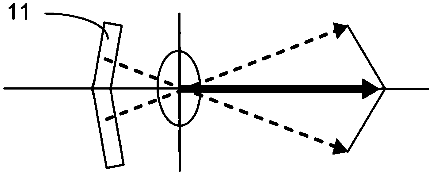
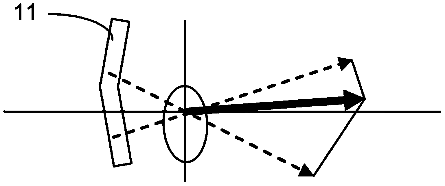
The invention relates to an array substrate, a manufacturing method of the array substrate and a liquid crystal display component. The array substrate comprises a lining substrate and a plurality of pixel units which are located on the lining substrate, wherein each pixel unit comprises a first electrode, a first insulating layer and a second electrode which are sequentially stacked, the first electrode is provided with an opening, an auxiliary electrode is arranged under the first electrode, the second electrode is V-shaped, and the projection of the corner of the V shape along the direction perpendicular to the lining substrate drops in the picture of the opening. The auxiliary electrode is added under the first electrode in the array substrate, the manufacturing method of the array substrate and the liquid crystal display component, the auxiliary electrode is opposite to the corner of the V shape of the second electrode, so that the auxiliary electrode can push liquid crystal molecules located at the corner position to rotate, and the disclination and pressing uneven phenomenon is improved.

Description

technical field [0001] The invention relates to the technical field of liquid crystal display, in particular to an array substrate, a manufacturing method thereof, and a liquid crystal display device using the array substrate. Background technique [0002] IPS mode and FFS mode are common liquid crystal display modes. The main feature of IPS mode and FFS mode is that the positive and negative electrodes are set on the same substrate, and the liquid crystal molecules rotate in the plane parallel to the substrate, so the light in each direction is uniform. It can pass through the short axis of liquid crystal molecules to achieve the purpose of wide viewing angle. At the same time, since the liquid crystal molecules in the IPS mode and the FFS mode are arranged horizontally, the deflection speed of the liquid crystal molecules is faster than that in the traditional vertical arrangement, so the response speed of the liquid crystal display device in the IPS mode and the FFS mode ...

Claims


Application Information

Patent Timeline
IPC IPC(8): G02F1/1343G02F1/1362H01L27/12H01L21/77
Inventor 叶岩溪沈柏平吴玲
Owner XIAMEN TIANMA MICRO ELECTRONICS
Why Eureka
Try Eureka