Wideband ceramic anti-metallic label

A broadband and tag technology, applied in the field of radio frequency identification and broadband ceramic anti-metal tags, can solve the problems of narrow antenna bandwidth and limit the use of tags, and achieve the effect of high Q value, prolonging the reading and writing distance, and widening the bandwidth

Inactive Publication Date: 2015-02-11
BEIJING CEC HUADA ELECTRONIC DESIGN CO LTD
View PDF3 Cites 5 Cited by
  • Summary
  • Abstract
  • Description
  • Claims
  • Application Information

AI Technical Summary

Problems solved by technology

However, due to the higher the dielectric constant of the ceramic medium, the larger the Q value, most of the energy is stored in the medium, and the bandwidth of the antenna is extremely narrow, only a few tenths of ordinary large-size anti-metal tags, which limits the use of tags. use

Method used


Image

  • Wideband ceramic anti-metallic label

Examples


Embodiment Construction

[0014] The specific embodiments described herein are only used to explain the present invention, and are not intended to limit the present invention.

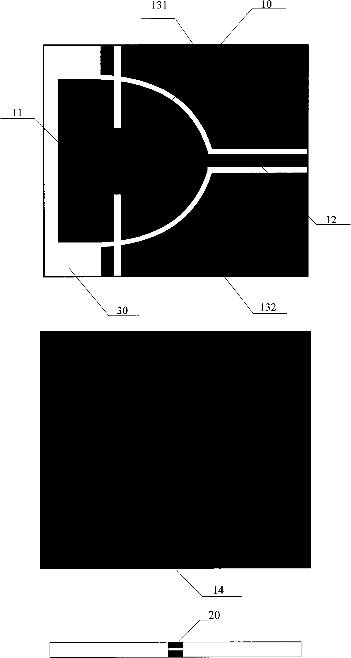
[0015] refer to figure 1 In this embodiment, the broadband ceramic anti-metal tag includes an antenna 10, a chip 20 and a substrate 30, the substrate 30 accommodates the antenna 10 and the chip 20, wherein the antenna 10 matches the chip 20, and the antenna 10 includes a radiating portion 11 , the impedance adjustment part 12 , the coplanar coupling part 13 and the ground plane 14 , the radiation part 11 , the impedance adjustment part 12 and the coplanar coupling part 13 are located on the front side of the substrate 30 , and the ground plane 14 is located on the back side of the substrate 30 , the chip 20 is located on the side of the substrate 30 and is connected to the impedance adjusting part 12 and the ground plane 13 .

[0016] The shape and size of the substrate 30 are specifically required to be set. For example, in ...


PUM


Abstract

The invention relates to the field of RFID (Radio Frequency Identification) and provides a wideband ceramic anti-metallic label. The wideband ceramic anti-metallic label is characterized by comprising an antenna, a chip and a base plate, wherein the base plate is used for containing the antenna and the chip, and the antenna and the chip are matched; the antenna comprises a radiating part, an impedance-regulating part, a coplanar coupling part and a grounding surface, wherein the radiating part, the impedance-regulating part and the coplanar coupling part are positioned on the front surface of the base plate, the grounding surface is positioned on the back surface of the base plate, and the chip is positioned on the lateral surface of the base plate; the chip is connected with the impedance-regulating part and the grounding surface. The ceramic anti-metallic label has a small size, the Q value and the broadening bandwidth of the antenna can be greatly decreased through the special design of the antenna, and the performance of the ceramic anti-metallic label is superior to that of an ordinary large-sized anti-metallic label, so that the ceramic anti-metallic label can be conveniently applied to many metal environments which have smaller sizes and simultaneously have higher requirements on reading distances and bandwidth.

Description

Technical field: [0001] The invention relates to a broadband ceramic anti-metal tag, belonging to the technical field of microwave communication and suitable for radio frequency identification in the frequency range of 800MHz to 1GHz Background technique: [0002] In recent years, with the development of RFID, more and more electronic tags are used in the fields of logistics and anti-counterfeiting. Ordinary flat paper labels attached to the metal surface have reduced radiation efficiency, impedance and radiation pattern changes, resulting in a significant decrease in the reading distance of such labels or even unreadability. Therefore, it is usually necessary to use anti-metal labels for metal environments. In recent years, ceramic anti-metal labels use ceramic materials with high dielectric constant as the substrate, which greatly reduces the size of the label and improves the performance of the label on metal objects, especially small-sized metal parts. on the usage rate...

Claims


Application Information

Patent Timeline
Patent Type & Authority Applications(China)
IPC IPC(8): G06K19/02G06K19/07
Inventor 秦津津马纪丰赵军伟
Owner BEIJING CEC HUADA ELECTRONIC DESIGN CO LTD
Why Eureka
Try Eureka