Method and system for detecting SAG signal in DVR device
A signal and sampling point technology, applied in the direction of measuring devices, measuring electrical variables, measuring current/voltage, etc., can solve problems such as large amount of calculation and delay in detection time, and achieve the effect of reducing time delay and saving calculation time
- Summary
- Abstract
- Description
- Claims
- Application Information
AI Technical Summary
Problems solved by technology
Method used
Image

Examples
Embodiment Construction
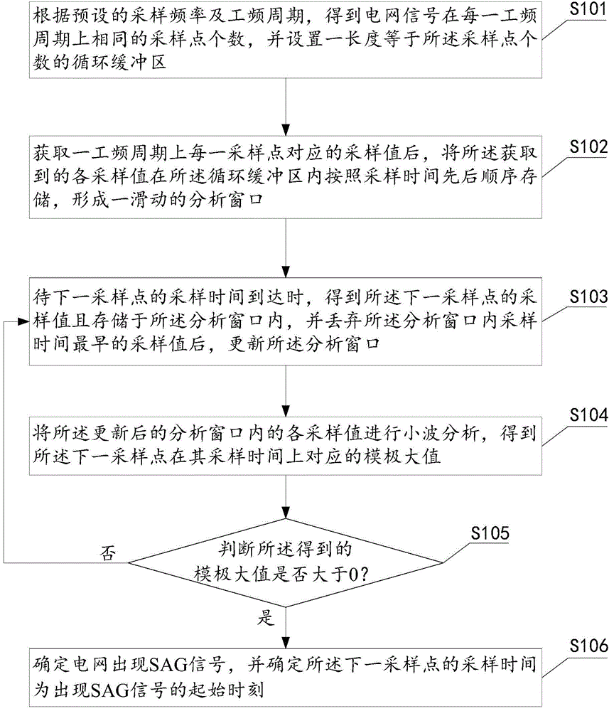
[0030] In order to make the object, technical solution and advantages of the present invention clearer, the present invention will be further described in detail below in conjunction with the accompanying drawings.
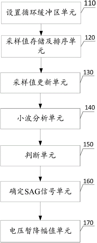
[0031] Such as figure 1 As shown, a method for detecting a SAG signal in a DVR device provided by an embodiment of the present invention, the method includes:
[0032] Step S101, according to the preset sampling frequency and power frequency cycle, obtain the same number of sampling points of the power grid signal in each power frequency cycle, and set a circular buffer whose length is equal to the number of sampling points;
[0033] The specific process is that the sampling frequency of the grid signal can be set to 6.4KHz, the power frequency cycle is set to 20ms or the sampling frequency is set to 12.8KHz, the power frequency cycle is set to 20ms and other special values, so that the sampling frequency within 20ms of each power frequency cycle The number of po...
PUM
 Abstract
Description
Claims
Application Information
 - R&D
- Intellectual Property
- Life Sciences
- Materials
- Tech Scout
- Unparalleled Data Quality
- Higher Quality Content
- 60% Fewer Hallucinations
Browse by: Latest US Patents, China's latest patents, Technical Efficacy Thesaurus, Application Domain, Technology Topic, Popular Technical Reports.
© 2025 PatSnap. All rights reserved.Legal|Privacy policy|Modern Slavery Act Transparency Statement|Sitemap|About US| Contact US: help@patsnap.com