Multilayer circuit board and manufacturing method thereof

A technology of a multilayer circuit board and a manufacturing method, which is applied in the direction of multilayer circuit manufacturing, printed circuit manufacturing, printed circuit, etc., can solve the problem of lifting and peeling of the gold-plated layer, the gold finger end of the circuit board cannot be smoothly inserted and removed, and the impact on the gold finger Electrical connection performance and other issues, to achieve the effect of improving plugging and unplugging

Active Publication Date: 2015-03-18
AVARY HLDG (SHENZHEN) CO LTD +1
View PDF12 Cites 7 Cited by
  • Summary
  • Abstract
  • Description
  • Claims
  • Application Information

AI Technical Summary

Problems solved by technology

When the gold finger end of the circuit board is plugged and pulled out with other electronic devices for many times, the gold plating layer remaining on the surface of the electroplated connection at the end of the conductive

Method used


Image

  • Multilayer circuit board and manufacturing method thereof
  • Multilayer circuit board and manufacturing method thereof
  • Multilayer circuit board and manufacturing method thereof

Examples


Example Embodiment

[0025] The multi-layer circuit board provided by the technical solution and the manufacturing method thereof will be further described in detail below with reference to the accompanying drawings and embodiments.

[0026] The manufacturing method of the multilayer circuit board provided by the embodiment of the technical solution includes the following steps:
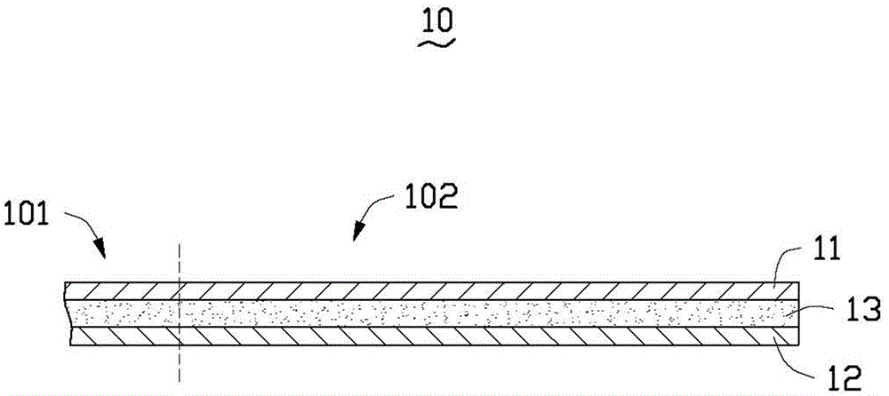
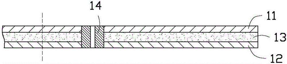
[0027] The first step, see figure 1 , Provide a circuit substrate 10, the circuit substrate 10 includes a first copper foil layer 11, a second copper foil layer 12 and at least one insulating layer 13 located between the first copper foil layer 11 and the second copper foil layer 12 The first copper foil layer 11 and the second copper foil layer 12 are respectively located on the outermost two sides of the circuit substrate 10.

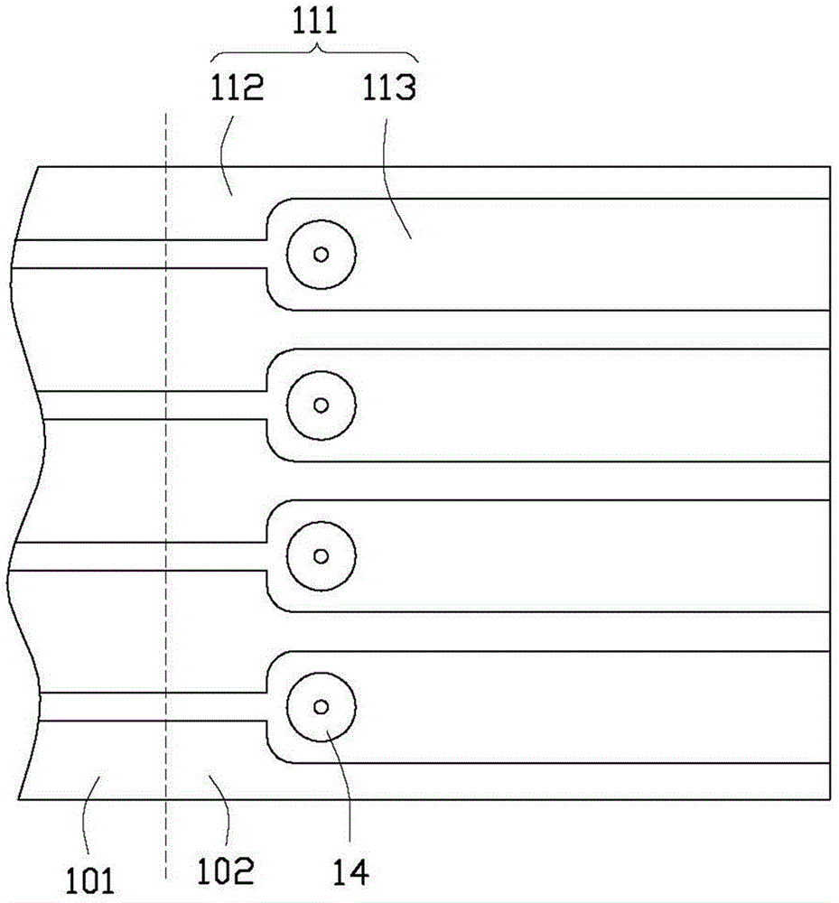
[0028] The circuit substrate 10 includes a first area 101 and a second area 102. The first area 101 is an area for subsequent wiring, and the second area 102 is an area for subsequent conductive termin...


PUM


Abstract

Disclosed is a manufacturing method of a multilayer circuit board. The method comprises the following steps: providing a circuit board substrate comprising a first copper foil layer and a second copper foil layer at outermost two sides, wherein the circuit board substrate comprises a second area; forming multiple conductive through holes electrically connected with the first copper foil layer and the second copper foil layer in the second area; manufacturing the first copper foil layer and the second copper foil layer to form a first conductive line pattern and a second conductive line pattern, wherein the first conductive line pattern comprises multiple conductive terminals in the second area, the second conductive line pattern comprises multiple electroplated connecting lines in the second area, and each conductive terminal is electrically connected with one electroplated connecting line through one conductive through hole; forming coverage film layers at the two sides of the circuit board substrate, wherein the coverage film layer disposed at the surface of the first conductive line pattern is provided with openings, and the multiple conductive terminals are exposed out of the openings; and forming a gold-plated layer on the surfaces of multiple conductive terminals. According to the invention, each electroplated connecting line is disconnected through a laser ablation mode, and the multilayer circuit board is formed accordingly. The invention also provides a multilayer circuit board formed by use of the manufacturing method of the multilayer circuit board.

Description

technical field [0001] The invention relates to circuit board manufacturing technology, in particular to a multilayer circuit board and a manufacturing method thereof. Background technique [0002] At present, many multilayer circuit boards are electrically connected to other electronic devices through gold fingers. Usually, the gold fingers are formed by chemical gold plating or electroplating on the surface of multiple conductive terminals of the circuit board after the circuit is formed. If it is formed in the form of gold, when forming lines on this circuit board, it is necessary to form a plurality of electroplating connections electrically connected to the conductive terminals at the same time as the ends of the plurality of conductive terminals (that is, the end close to the edge of the product). The wire is used for electrical connection with the electroplating device. After the electroplating is completed, the electroplating wire is cut by punching to form a finishe...

Claims


Application Information

Patent Timeline
IPC IPC(8): H05K3/46H05K1/02H05K1/11
CPCH05K1/116H05K3/46H05K2203/0703
Inventor 苏威硕
Owner AVARY HLDG (SHENZHEN) CO LTD
Why Eureka
Try Eureka