

On-chip integrated beam combining laser based on photonic crystal y-waveguide and manufacturing method thereof
A photonic crystal and two-dimensional photonic crystal technology, which is applied to the structure of optical waveguide light guide and optical waveguide semiconductor, can solve the problem that the semiconductor laser unit device cannot balance high output power and high beam quality well, and avoid the interface Loss, cost and difficulty reduction, compactness effect
- Summary
- Abstract
- Description
- Claims
- Application Information
AI Technical Summary
Problems solved by technology
Method used
Image

Examples
Embodiment
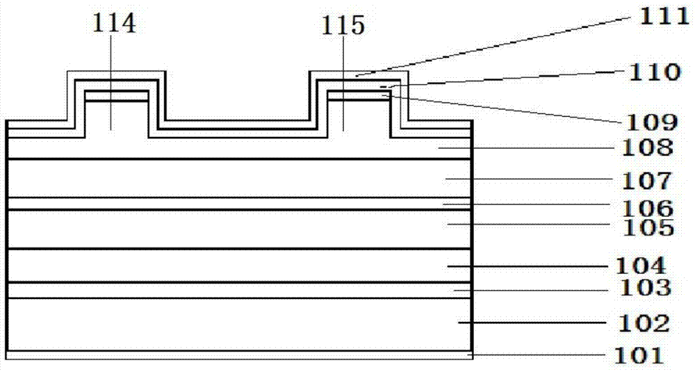
[0049] A method for manufacturing an on-chip integrated beam combining laser based on a photonic crystal Y-waveguide, comprising the steps of:
[0050] Step 1, select a GaAs substrate 102; grow a 300nm n-type GaAs buffer layer 103 and a 1500nm Al0.6Ga0.4As n-type cladding layer 104 sequentially on the n-type GaAs substrate 102 by metal-organic chemical vapor deposition , 150nm Al0.3Ga0.7As lower waveguide layer 105, 10nm InGaAlAs single quantum well 106, 150nm Al0.3Ga0.7As upper waveguide layer 107, 1500nm Al0.6Ga0.4As p-type cladding layer 108 and 200nm p-type heavy Doping the capping layer 109, the excitation wavelength of the obtained epitaxial wafer is 808nm;
[0051]Step 2, cleaning the epitaxial wafer with acetone, ethanol, isopropanol;
[0052] Step 3, coating photoresist on the washed epitaxial wafer, then exposing and developing;
[0053] Step 4, using the method of inductively coupled ion etching, etch the p-type cladding layer 109 down to the p-type cladding layer...
PUM
 Abstract
Description
Claims
Application Information