Circuit and method capable of lowering loop noise of active earphone
An earphone and loop technology is applied in the field of circuits for reducing the loop noise of active earphones, which can solve the problems of magnetic field radiation, easy generation of loop current, and magnetic field interference of speakers, so as to achieve low magnetic field radiation and reduce active earphone loops. effect of noise
- Summary
- Abstract
- Description
- Claims
- Application Information
AI Technical Summary
Problems solved by technology
Method used
Image
Examples
Embodiment 1
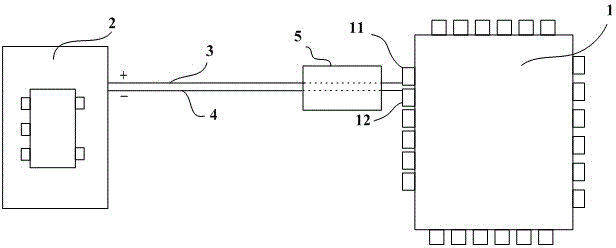
[0026] Embodiment one, see figure 1 As shown, the circuit for reducing loop noise in this embodiment includes an integrated circuit module 1 and a power supply module 2 . The integrated circuit module 1 may be an integrated circuit that realizes radio frequency transceiver function. The power supply module 2 supplies power to the integrated circuit module 1 through a power line 3 drawn out from the power supply module 2 . The ground wire 4 is arranged in parallel with the power wire 3. In order to filter the high-frequency noise in the circuit and cut off the transmission path of the high-frequency noise through the power supply circuit, a filter capacitor 5 is also connected between the power line 3 and the ground line 4 . The filter capacitor 5 is arranged on one side of the integrated circuit module 1 . In the prior art, the filter capacitor 5 is often connected in parallel between the signal line and the ground line to bypass the high-frequency noise. However, due to t...
Embodiment 2
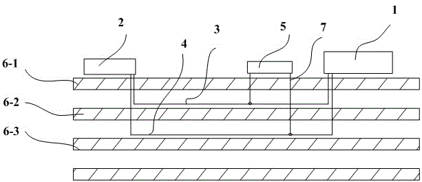
[0030] Embodiment 2. Due to the limited space in the ear shell of the active earphone, the PCB used in another embodiment of the present invention is a four-layer board. Such as figure 2 As shown, the integrated circuit module 1, the power supply module 2 and the filter capacitor 5 are arranged on the first layer 6-1 of the PCB, and the power line 3 is arranged on the second layers 6-2, 6-1 and 6-1 of the PCB. 2 is the signal layer of the PCB; the ground wire is laid on the third layer 6-3 of the PCB, that is, the ground layer of the PCB. A plurality of via holes 7 for connecting the power line 3 and the ground line 4 are opened on the PCB. The via hole 7 has the smallest distributed inductance, and its main function is to provide the shortest return path for the power line 3 and the ground line 4 . Through the via hole 7, the power line 3 is electrically connected to one pole of the filter capacitor 5 and the power pin 1-1 of the integrated circuit module 1; the ground lin...
PUM
 Abstract
Description
Claims
Application Information

