Test circuit, array substrate and display device

A technology for testing circuits and array substrates. It is applied in the field of display devices and testing circuits. It can solve problems such as jitter and image afterimages, and achieve the effects of avoiding polarization and accelerating dissipation.

Active Publication Date: 2015-04-01
XIAMEN TIANMA MICRO ELECTRONICS +1
View PDF6 Cites 14 Cited by
  • Summary
  • Abstract
  • Description
  • Claims
  • Application Information

AI Technical Summary

Problems solved by technology

[0004] The technical problem to be solved by the embodiments of the present invention is the problem of afterimage and jitter on the screen caused by sudden power failure in the electrical test in the prior art

Method used


Image

  • Test circuit, array substrate and display device
  • Test circuit, array substrate and display device
  • Test circuit, array substrate and display device

Examples


Embodiment Construction

[0025] In order to make the above objects, features and advantages of the present invention more comprehensible, specific implementations of the present invention will be described in detail below in conjunction with the accompanying drawings.

[0026] In the following description, many specific details are set forth in order to fully understand the present invention, but the present invention can also be implemented in other ways than those described here, so the present invention is not limited by the specific embodiments disclosed below.

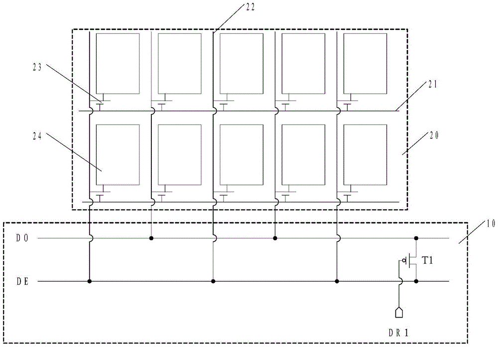
[0027] Such as figure 2 As shown, the embodiment of the present invention provides a test circuit 10 for testing a pixel array 20 including a plurality of data lines 22, including a first test bus DO, a second test bus DE and at least one first transistor T1; A test bus DO and a second test bus DE are respectively used to provide different test signals to different data lines in the plurality of data lines 22 . The first test bus DO and...


PUM


Abstract

The invention provides a test circuit. The test circuit is used for testing a pixel array comprising a plurality of data lines. The test circuit comprises a first test bus, a second test bus and at least one first transistor, wherein the first test bus and the second test bus are respectively used for providing different test signals for different data lines in the data lines; a grid electrode of each first transistor is electrically connected to a control terminal, a first pole of each first transistor is electrically connected with the first test bus, and a second pole of each first transistor is electrically connected with the second test bus; the first transistors are in a closed state in a test phase. The invention further provides an array substrate and a display device, and the test circuit provided by the invention is arranged on one side of the pixel array. Through the adoption of the test circuit and the array substrate provided by the invention, liquid crystal polarization caused by power failure can be avoided, and the problems of picture residual image and picture flutter are solved.

Description

technical field [0001] The present invention relates to the display field, in particular to a test circuit, an array substrate including the test circuit, and a display device including the array substrate. Background technique [0002] In recent years, active matrix display devices have been popularized, and are widely used in mobile devices such as mobile phones, tablet computers, MP3, and MP4, for example. In order to ensure the quality of the product, the display panel will generally undergo an electrical test before leaving the factory. figure 1 The testing method in the prior art is shown. Such as figure 1 As shown, it includes a pixel array 20 and two test lines DO and DE for testing the pixel array 20. The pixel array 20 includes a plurality of scanning lines 12, a plurality of data lines 13 and a plurality of switching devices 14; the pixel electrode 15 is located at the scanning The intersection of the lines 12 and the data lines 13 defines pixel areas, which ar...

Claims


Application Information

Patent Timeline
Patent Type & Authority Applications(China)
IPC IPC(8): G09G3/00G02F1/13
Inventor 苏俊雄吴昊
Owner XIAMEN TIANMA MICRO ELECTRONICS
Why Eureka
Try Eureka