Micro-fluidic chip having nano dendrite Raman substrate and manufacturing method thereof

A microfluidic chip and Raman substrate technology, applied in Raman scattering, chemical instruments and methods, laboratory utensils, etc., can solve problems such as failure to meet use requirements, low SERS activity, and low detection efficiency, and achieve savings Cost, simplified preparation process, effect of high SERS activity

Active Publication Date: 2015-04-08
TAIYUAN UNIV OF TECH
View PDF5 Cites 18 Cited by
  • Summary
  • Abstract
  • Description
  • Claims
  • Application Information

AI Technical Summary

Problems solved by technology

[0003] At present, the common method of combining SERS technology with microfluidic chips is to prefabricate the SERS substrate first, and then transfer the substrate to the working position, and these two steps virtually increase the time and cost of the process. In addition, in order to realize detection , the Raman substrate generally works inside the microfluidic channel, so the above two-step method will bring many difficulties to the subsequent bonding and packaging process; in order to solve this problem, electrodynamics, optical tweezers, nano-channel methods, etc. The enrichment method based on colloidal particles is widely used. However, because the colloidal particles in the liquid environment are very easy to adhere and agglomerate, these techniques have problems such as low detection efficiency and weak signal intensity. The SERS activity of the control chip is low, and it cannot meet the use requirements in many applications; The method of fixed-point and directional preparation of Raman substrates in microfluidic channels is particularly important

Method used


Image

  • Micro-fluidic chip having nano dendrite Raman substrate and manufacturing method thereof
  • Micro-fluidic chip having nano dendrite Raman substrate and manufacturing method thereof
  • Micro-fluidic chip having nano dendrite Raman substrate and manufacturing method thereof

Examples


Embodiment Construction

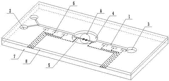
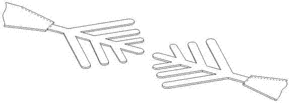
[0015] like figure 1 As shown, there is a microfluidic chip with a nanodendritic Raman substrate, the chip is provided with at least one microfluidic channel 1, and one end of the microfluidic channel 1 is provided with at least one sample pool 2, and each sample pool 2 is It communicates with the micro-channel 1 but does not communicate with each other. The other end of the micro-channel 1 is provided with at least one waste liquid pool 3, and each waste liquid pool 3 is connected with the micro-channel 1 but not connected to each other. Not connected, the micro-channel 1 is provided with at least one growth pool 4, and the micro-channel 1 passes through each growth pool 4, and at least one pair of first growth pools with tips are arranged in the growth pool 4. Electrodes 5, the two first electrodes 5 in each pair have the nano-dendrite structure of noble metal on the nearest tip, the noble metal is gold, platinum or palladium, the two first electrodes in each pair The dista...


PUM


Abstract

The invention relates to a micro-fluidic chip having a nano dendrite Raman substrate and a manufacturing method thereof. A solved technical problem is characterized in that the micro-fluidic chip with high SERS directly prepared in a micro channel and having the nano dendrite Raman substrate activity and the manufacturing method thereof. The technical scheme is characterized in that the micro-fluidic chip comprises a micro fluidic chip having the nano dendrite Raman substrate, at least a micro channel is arranged on the micro fluidic chip, at least a sample pool is arranged at one end of the micro channel, each sample pool and the micro channel are communicated, but the sample pools are not communicated with each other, at least a waste liquid pool is arranged at the other end of the micro channel, each waste liquid pool is communicated to the micro channel, but the waste liquid pools are not communicated with each other, at least a growth pool is arranged on the micro channel, the micro channel passes through each growth pool, at least a pair of first electrodes having tips are arranged in the growth pool, and a nano dendrite structure of precious metals is provided on tip of nearest distance between two first electrodes. The micro-fluidic chip is suitable for the technical filed of micro fluidic chip.

Description

technical field [0001] The invention belongs to the technical field of microfluidic chips, and in particular relates to a microfluidic chip with a nano-dendritic Raman substrate and a manufacturing method thereof. Background technique [0002] Surface-enhanced Raman scattering (SERS) technology can obtain information on the influence of genes, chemical bonds, and microenvironment on the structure of samples from the molecular level, and obtain its fingerprints in real time. , no damage, real-time detection and other characteristics, and will not be interfered by media such as solutions. Therefore, since it was discovered in 1974, SERS has been widely used in biochemical detection due to the above advantages; microfluidic chips are an application The core technology in the field of micro-analysis system, because of its small size, low cost, small reagent consumption, fast and efficient, easy integration and automation, etc., has great application potential in the fields of bi...

Claims


Application Information

Patent Timeline
Patent Type & Authority Applications(China)
IPC IPC(8): B01L3/00G01N21/65
Inventor 冀健龙乔畅李朋伟桑胜波张文栋
Owner TAIYUAN UNIV OF TECH
Why Eureka
Try Eureka