A direct type backlight module for pcb and its application

A backlight module, direct type technology, applied in the field of direct type backlight modules, can solve the problem of uneven lamp shadow display, and achieve the effect of weakening lamp shadow phenomenon, low cost, and improving optical taste

Active Publication Date: 2018-06-26
ANHUI COREACH TECH
View PDF11 Cites 0 Cited by
  • Summary
  • Abstract
  • Description
  • Claims
  • Application Information

AI Technical Summary

Problems solved by technology

[0004] The purpose of the present invention is to solve the technical problems of lamp shadows and uneven display caused by the use of traditional and black circle PCBs in existing direct-lit backlight modules

Method used


Image

  • A direct type backlight module for pcb and its application
  • A direct type backlight module for pcb and its application
  • A direct type backlight module for pcb and its application

Examples


Embodiment 1

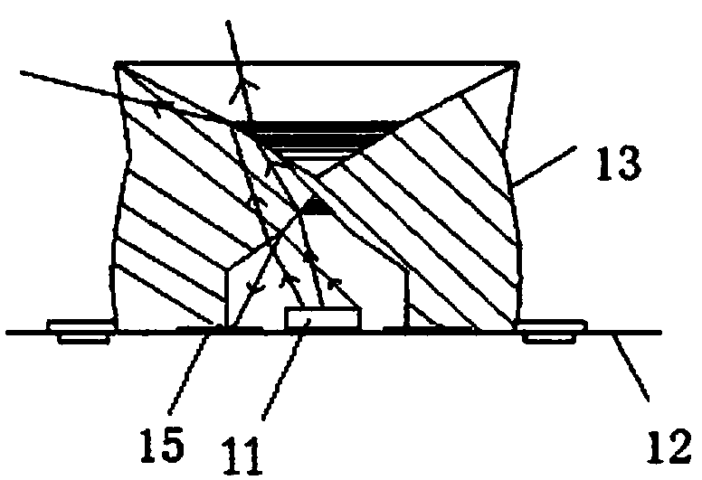
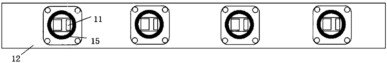
[0024] Such as Image 6 As shown, a PCB used in a direct type backlight module is characterized in that the upper surface of the solder mask layer of the PCB 12 has a plurality of dots 14 arranged in layers with the LED pad 17 as the center. The distribution range of 14 is limited to the secondary optical lens silk screen 16 on the PCB 12. The secondary optical lens screen 16 is the position where the secondary optical lens 13 is installed on the PCB 12, and the outlets 14 are distributed in the secondary optical lens screen 16 to enable the outlets 14 of all facilities to play an effective role. The shape of the distribution range of the dots 14 is circular, and the diameter of the dots 14 is 0.5 mm. The dots 14 around the LED pad 17 absorb light unevenly, which can weaken the light near the LED lamp 11, and relatively improve the reflection of light away from the LED lamp 11, thereby making the backlight module using the PCB more light. Evenly. The dots 14 are selective to ...

Embodiment 2

[0026] Such as Figure 7 As shown, a PCB used in a direct type backlight module is characterized in that a plurality of dots 14 are provided on the upper surface of the solder resist layer of the PCB 12, and the dots 14 are arranged in layers with the LED pad 17 as the center. The distribution range of 14 is limited to the secondary optical lens silk screen 16 on the PCB 12. The secondary optical lens screen 16 is a position on the PCB 12 where the secondary optical lens 13 is installed, and the outlets 14 are distributed in the secondary optical lens screen 16 to enable the outlets 14 of all facilities to play an effective role. The shape of the distribution range of the dots 14 is square, and the diameter of the dots 14 is 1.5 mm. The dots 14 around the LED pad 17 absorb light unevenly, which can weaken the light near the LED lamp 11, and relatively improve the reflection of light away from the LED lamp 11, thereby making the backlight module using the PCB more light. Evenly...

Embodiment 3

[0028] Such as Picture 8 As shown, a PCB is used in a direct-lit backlight module. The upper surface of the solder mask of PCB 12 has a plurality of dots 14. The dots 14 are arranged in layers with the LED pad 17 as the center. The distribution range of the dots 14 It is limited to the secondary optical lens silk screen 16 on the PCB 12. The secondary optical lens screen 16 is the position where the secondary optical lens 13 is installed on the PCB 12, and the outlets 14 are distributed in the secondary optical lens screen 16 to enable the outlets 14 of all facilities to play an effective role. The shape of the distribution range of the dots 14 is a rhombus, and the diameter of the dots 14 is 2 mm. The dots 14 around the LED pad 17 absorb light unevenly, which can weaken the light near the LED lamp 11, and relatively improve the reflection of light away from the LED lamp 11, thereby making the backlight module using the PCB more light. Evenly. The dots 14 are selective to li...


PUM

PropertyMeasurementUnit
diameteraaaaaaaaaa
diameteraaaaaaaaaa
diameteraaaaaaaaaa

Abstract

The invention discloses a PCB and a direct type backlight module with the PCB and relates to the technical field of backlight. The PCB is provided with multiple network points. The network points are arranged layer by layer with LEDs serving as the centers and limited within the lens screen printing range. The direct type backlight module comprises a lamp bar. The lamp bar is composed of lenses, the LEDs and the PCB. Compared with the prior art, the PCB and the direct type backlight module have the following advantages that different network points and arrangement modes can be adopted according to actual requirements, the optical level of the direct type backlight module can be effectively improved, the lamp shadow phenomenon is weakened, cost is reduced, the scheme of the PCB and the direct type backlight module is simple, cost is low, the lamp shadow problem can be effectively solved, illumination evenness is improved, and the cost of the backlight module can be greatly reduced.

Description

Technical field [0001] The invention relates to the technical field of backlights of liquid crystal displays, in particular to a PCB and a direct-lit backlight module used by the PCB, which improves optical taste and improves the display effect of the backlight module. Background technique [0002] With the introduction of energy conservation and environmental protection policies, LED LCD TVs have gradually replaced traditional CRT TVs, occupying more and more markets. With the gradual reduction of the module's light mixing distance, the uneven light irradiated on the LCD panel results in the phenomenon of lamp shadow. The problem of lamp shadow has become a resistance to the ultra-thin backlight module. There are two traditional solutions for lamp shadow. One is to increase the number of diaphragms, but the cost will increase; the other is to draw a black circle on the PCB. Although this method can weaken part of the lamp shadow, the black circle absorbs more light, causing the ...

Claims


Application Information

Patent Timeline
Patent Type & Authority Patents(China)
IPC IPC(8): F21V19/00F21S8/00G02F1/13357F21Y115/10
CPCF21S8/00F21V19/001F21V19/005
Inventor 杨周彭友陈龙年靠江陈宝
Owner ANHUI COREACH TECH
Why Eureka
Try Eureka