Restoration method of DRAM (Dynamic Random Access Memory) chip

A repair method and chip technology, applied in static memory, instruments, etc., can solve the problems of not being able to guarantee the robustness of chip test results, not being able to truly reflect chip designers, etc., and achieve the effect of ensuring correct access

Active Publication Date: 2015-04-29
XI AN UNIIC SEMICON CO LTD
View PDF4 Cites 4 Cited by
  • Summary
  • Abstract
  • Description
  • Claims
  • Application Information

AI Technical Summary

Problems solved by technology

[0004] In order to solve the existing use of 2 n The method that the number of addresses is the boundary cannot truly reflect the needs of chip designers, and the writing of the topology cannot guarantee the robustness of the chip test results. The present invention provides a method for finding the address boundary of a DRAM chip.

Method used


Image

  • Restoration method of DRAM (Dynamic Random Access Memory) chip
  • Restoration method of DRAM (Dynamic Random Access Memory) chip

Examples


Embodiment Construction

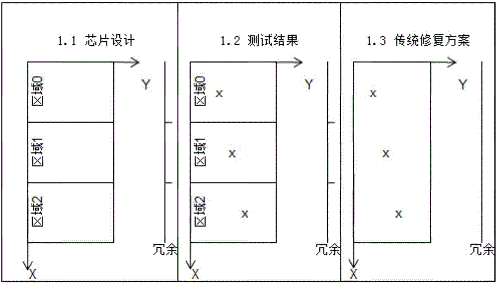
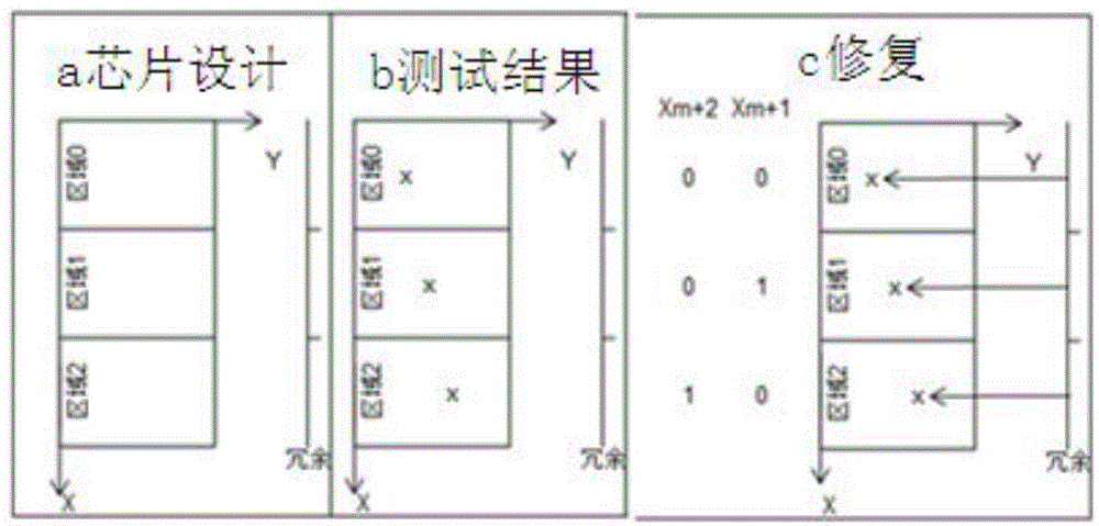
[0017] Taking the repair of DRAM chips as an example, it demonstrates the application of address boundary positioning in DRAM repair, as an example of trisection.

[0018] Such as figure 2 As shown, the repair plan provided by the chip designer is given in a, assuming that the DRAM has m (m is equal to an integer) bit X address, that is, the number of X addresses of the chip is 2 m and 2 m addresses are evenly distributed in 3 independent repair areas (area 0, area 1 and area 2), so the number of X addresses for each independent repair area is 2 m / 3, a redundant storage unit is also divided into three equal storage units according to the same rule, and each divided storage unit can independently repair the failure address of a repair area (using storage redundancy within the respective repair boundaries unit to repair the failed unit). As shown in part c, for the situation that the chip is divided into three equal parts in the X direction, on the basis of the m-bit X addr...


PUM


Abstract

The invention relates to a restoration method of a DRAM (Dynamic Random Access Memory) chip. The restoration method comprises the following steps of: adopting a method for expanding virtual address bits, loading non-2n (n is equal to an integer) addresses into the expanded virtual address bits, and using the virtual address bits to carry out identification on the boundaries of the chip designing addresses. The restoration method has the advantages that the need of chip designing persons is really reflected, so that a series of problems related to positioning of the address boundaries in chip testing are solved; and since the two expanded virtual addresses can not generate any influence on the X address of the original m-bit chip, the normal addressing of the chip is not influenced and further correct access for the address of the test chip is guaranteed.

Description

technical field [0001] The invention relates to a method for repairing a DRAM chip. Background technique [0002] When the design of DRAM chips is no longer based on the traditional 2 n When (n is equal to an integer) number of addresses is the design boundary, the test instrument will not be able to locate the design boundary of the chip. The existing solution is to abandon the real address boundary of the chip and still use 2 n The number of addresses is the boundary. This approach cannot truly reflect the needs of chip designers, which in turn leads to a series of problems related to address boundary positioning in chip testing, such as: DRAM chip repair solutions cannot be implemented, topology writing cannot guarantee the accuracy of chip test results, etc. . [0003] Such as figure 1 as shown, figure 1 1.1 in 1 gives the repair plan provided by the chip designer, assuming that the DRAM has m (m is equal to an integer) bit X address, that is, the number of X addres...

Claims


Application Information

Patent Timeline
IPC IPC(8): G11C29/44
Inventor 王正文
Owner XI AN UNIIC SEMICON CO LTD
Why Eureka
Try Eureka