Solid-state imaging device
A solid-state imaging device and pixel technology, which is applied in the fields of electric solid-state devices, radiation control devices, image communication, etc., can solve the problems of signal-to-noise ratio deterioration and signal volume reduction.
- Summary
- Abstract
- Description
- Claims
- Application Information
AI Technical Summary
Problems solved by technology
Method used
Image

Examples
no. 1 approach
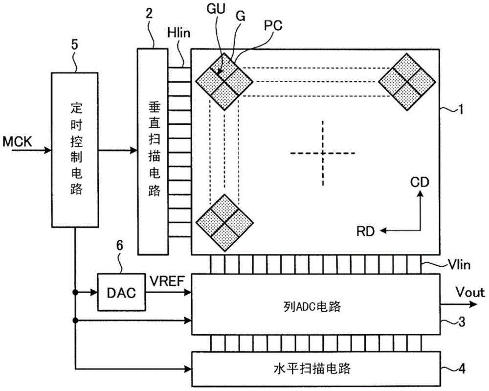
[0037] figure 1 It is a block diagram showing a schematic configuration of the solid-state imaging device of the first embodiment.
[0038] exist figure 1 Among them, the solid-state imaging device is provided with: a pixel array unit 1, in which pixels PC storing charges obtained by photoelectric conversion are arranged in a matrix along the row direction RD and column direction CD; The pixel PC of the read object; the column ADC circuit 3, which uses CDS to detect the signal component of each pixel PC; the horizontal scanning circuit 4, which scans the pixel PC of the read object along the horizontal direction; the timing control circuit 5, which controls the readout of each pixel PC or accumulation timing; and the reference voltage generation circuit 6 outputs the reference voltage VREF to the column ADC circuit 3 . Furthermore, the timing control circuit 5 is input with a master clock MCK.
[0039] In addition, in the pixel array section 1, a horizontal control line Hli...
no. 2 approach
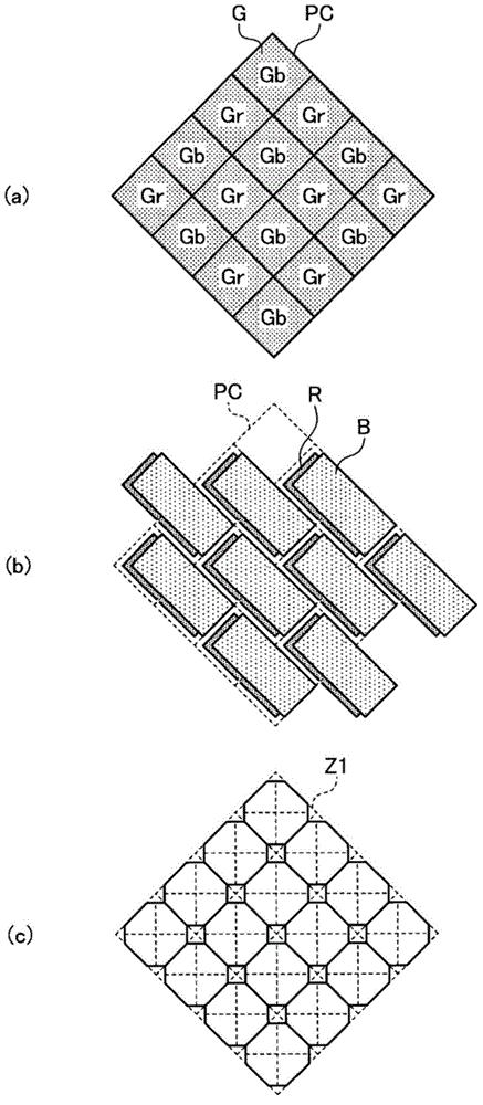
[0081] Figure 12 It is a plan view showing a layout example of photodiodes, floating diffusion regions, and gate electrodes of the solid-state imaging device according to the second embodiment.
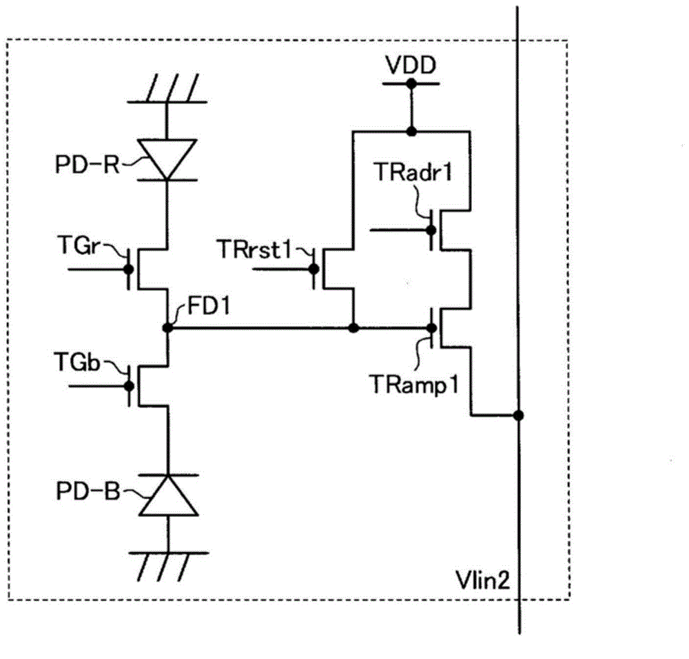
[0082] exist Figure 5 In the configuration shown in , the photodiodes PD-R and PD-B are arranged so as to overlap in the depth direction across two pixels.
[0083] while in Figure 12 Here, photodiodes PD-R and PD-B are provided individually for each pixel. Here, the photodiodes PD-R and PD-B can be alternately arranged for each pixel.
no. 3 approach
[0085] Figure 13 It is a plan view showing a layout example of photodiodes, floating diffusion regions, and gate electrodes of the solid-state imaging device according to the third embodiment.
[0086] exist Figure 12 In the configuration shown in , the floating diffusion FD is shared between two adjacent pixels in the oblique direction.
[0087] On the other hand, in Figure 13 In this case, the floating diffusion region FD is shared between two adjacent pixels along the column direction CD.
PUM
 Abstract
Description
Claims
Application Information
 - R&D
- Intellectual Property
- Life Sciences
- Materials
- Tech Scout
- Unparalleled Data Quality
- Higher Quality Content
- 60% Fewer Hallucinations
Browse by: Latest US Patents, China's latest patents, Technical Efficacy Thesaurus, Application Domain, Technology Topic, Popular Technical Reports.
© 2025 PatSnap. All rights reserved.Legal|Privacy policy|Modern Slavery Act Transparency Statement|Sitemap|About US| Contact US: help@patsnap.com