Array substrate, display device and image display method

An array substrate and image display technology, applied in static indicators, nonlinear optics, instruments, etc., can solve problems such as display brightness differences and poor horizontal stripes on flat panel displays, reduce charging differences, improve horizontal stripes, reduce The effect of small display brightness differences

Active Publication Date: 2017-06-30
BOE TECH GRP CO LTD +1
View PDF5 Cites 0 Cited by
  • Summary
  • Abstract
  • Description
  • Claims
  • Application Information

AI Technical Summary

Problems solved by technology

When there is a jump in the voltage loaded on the data line 102, due to the certain resistance of the data line 102 itself, the voltage loaded on the data line 102 will charge the sub-pixels of each row differently, which will cause the display brightness of the sub-pixels of each row to be different. There is a difference, which will lead to serious horizontal stripes when the flat panel monitor displays the picture

Method used


Image

  • Array substrate, display device and image display method
  • Array substrate, display device and image display method
  • Array substrate, display device and image display method

Examples


example 1

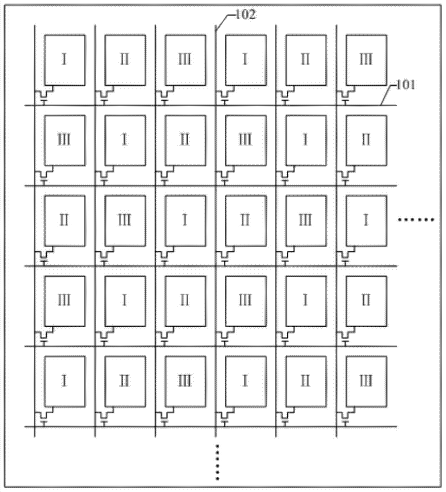
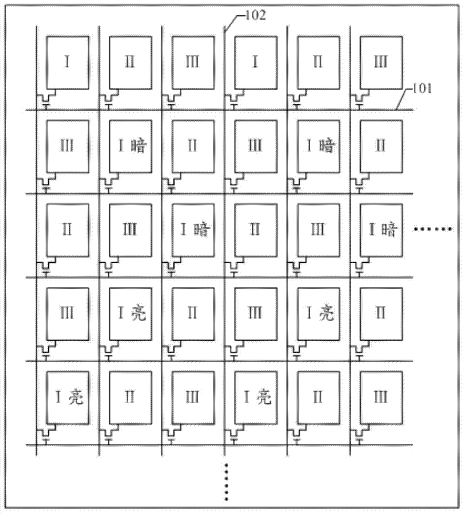
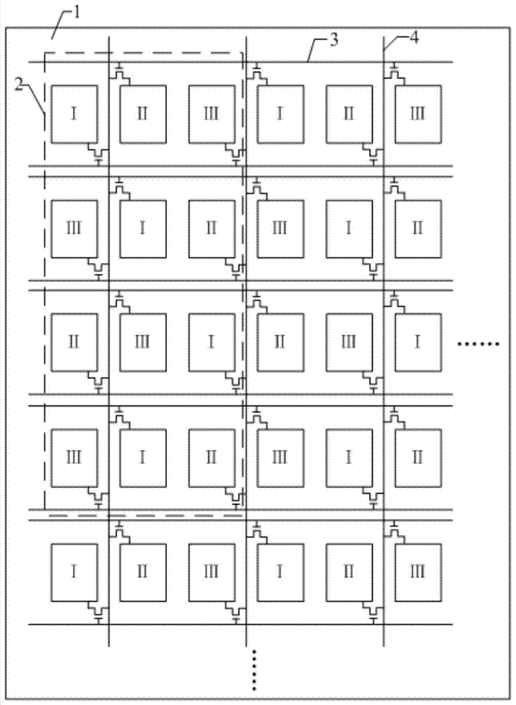
[0056] Example 1: The color resistance color of the first sub-pixel I is green (G), the color resistance colors of the second sub-pixel II and the third sub-pixel III are red (R) and blue (B), respectively, then as image 3 The arrangement of each sub-pixel in the array substrate shown corresponds to the following Figure 4 The arrangement shown; the first gray scale displayed for each first sub-pixel I, that is, each sub-pixel G is smaller than the second gray scale displayed for each second sub-pixel II, that is, each sub-pixel R, and each first sub-pixel I, namely The first gray scale displayed by each sub-pixel G is larger than the third gray scale displayed by each third sub-pixel III, that is, the third gray scale displayed by sub-pixel B, which can improve the horizontal streak defect.

[0057] Such as Figure 4 As shown, in the sub-pixels in the second row, the voltage of the sub-pixel G located in the second column jumps from the voltage of the sub-pixel G located in...

example 2

[0061] Example 2: the color resistance color of the second sub-pixel II is green (G), and the color resistance colors of the first sub-pixel I and the third sub-pixel III are red (R) and blue (B); image 3 The arrangement of each sub-pixel in the array substrate shown corresponds to the following Figure 6 The arrangement shown; the second gray scale displayed for each second sub-pixel II, that is, each sub-pixel G is greater than the first gray scale displayed for each first sub-pixel I, that is, each sub-pixel R, and each second sub-pixel II, namely The second gray scale displayed by each sub-pixel G is smaller than the third gray scale displayed by each third sub-pixel III, that is, the third gray scale displayed by sub-pixel B, which can improve the horizontal streak defect.

[0062] Such as Figure 6 As shown, in the second row of sub-pixels, the voltage of sub-pixel G located in the third column jumps from the voltage of sub-pixel B located in the fourth column of the s...

example 3

[0066] Example 3: the color resistance color of the third sub-pixel III is green (G), and the color resistance colors of the first sub-pixel I and the second sub-pixel II are red (R) and blue (B); image 3 The arrangement of each sub-pixel in the array substrate shown corresponds to the following Figure 8 The arrangement shown; the third gray scale displayed for each third sub-pixel III, that is, each sub-pixel G is smaller than the first gray scale displayed for each first sub-pixel I, that is, each sub-pixel R, and each third sub-pixel III is The third gray scale displayed by each sub-pixel G is larger than the second gray scale displayed by each second sub-pixel II, that is, the sub-pixel B, which can improve the horizontal stripe defect.

[0067] Such as Figure 8 As shown, in the sub-pixels in the second row, the voltage of the sub-pixel G located in the first column jumps from the voltage of the sub-pixel R located in the second column of the second row, and the voltag...


PUM


Abstract

The invention discloses an array substrate, a display device and an image display method. In the array substrate, each sub-pixel is divided into a group by two adjacent columns of sub-pixels, and the sub-pixels in each group do not overlap each other; Each sub-pixel in each group is electrically connected to the same data line; each row of sub-pixels corresponds to two gate lines, and the two sub-pixels belonging to the same group in each row of sub-pixels are respectively connected to the two gate lines corresponding to the row of sub-pixels Electrically connected; in this way, during the process of sequentially loading the gate scanning signal to each gate line within the display time of one frame, the charging difference of each row of sub-pixels caused by the jump of the voltage loaded on the data line can be reduced , so that the difference in display brightness of the sub-pixels in each row can be reduced, and the defect of horizontal stripes existing in the display screen of the flat panel display can be improved.

Description

technical field [0001] The present invention relates to the field of display technology, in particular to an array substrate, a display device and an image display method. Background technique [0002] With the continuous development of display technology, flat panel displays such as Organic Light Emitting Diode (OLED), Plasma Display Panel (PDP) and Liquid Crystal Display (LCD) are developing rapidly. [0003] Taking the existing LCD as an example for illustration, on the side of the array substrate in the existing LCD, such as figure 1 As shown, a plurality of gate lines 101 and a plurality of data lines 102 intersecting and insulated from each other are generally provided, as well as a plurality of sub-pixels (I, II, III). I, II, and III can represent red (R), green Either color of (G) and blue (B). Such as figure 1 As shown, in each column of sub-pixels, the color resistance colors of every two adjacent sub-pixels are different. When the gate lines 101 are sequential...

Claims


Application Information

Patent Timeline
Patent Type & Authority Patents(China)
IPC IPC(8): G02F1/1362
CPCG09G3/3607G09G2300/0426G09G2300/0452G09G2320/0233G09G2320/0242
Inventor 王凯旋李伟袁洪亮刘建涛王迎姿马振富
Owner BOE TECH GRP CO LTD
Why Eureka
Try Eureka